Article

Investigation of HfO2 Thin Films on Si by X-ray Photoelectron Spectroscopy, Rutherford Backscattering, Grazing Incidence X-ray Diffraction and Variable Angle Spectroscopic Ellipsometry

1
Laboratory of Optoelectronic Materials & Detection Technology, Guangxi Key Laboratory for the Relativistic Astrophysics, School of Physical Science & Technology, Guangxi University, Nanning 530004, China
2
School of Physical Science & Technology, Guangxi University, Nanning 530004, China
3
Department of Electrical Engineering, Graduate Institute of Electronics Engineering, National Taiwan University, Taipei 106-17, Taiwan
4
State Key Laboratory of Nuclear Physics and Technology, Peking University, Beijing 100871, China
*
Authors to whom correspondence should be addressed.
Crystals 2018, 8(6), 248; https://doi.org/10.3390/cryst8060248
Submission received: 23 April 2018 / Revised: 31 May 2018 / Accepted: 5 June 2018 / Published: 12 June 2018
(This article belongs to the Special Issue Functional Oxide Based Thin-Film Materials)

Abstract

:
Hafnium oxide (HfO2) thin films have been made by atomic vapor deposition (AVD) onto Si substrates under different growth temperature and oxygen flow. The effect of different growth conditions on the structure and optical characteristics of deposited HfO2 film has been studied using X-ray photoelectron spectroscopy (XPS), Rutherford backscattering spectrometry (RBS), grazing incidence X-ray diffraction (GIXRD) and variable angle spectroscopic ellipsometry (VASE). The XPS measurements and analyses revealed the insufficient chemical reaction at the lower oxygen flow rate and the film quality improved at higher oxygen flow rate. Via GIXRD, it was found that the HfO2 films on Si were amorphous in nature, as deposited at lower deposition temperature, while being polycrystalline at higher deposition temperature. The structural phase changes from interface to surface were demonstrated. The values of optical constants and bandgaps and their variations with the growth conditions were determined accurately from VASE and XPS. All analyses indicate that appropriate substrate temperature and oxygen flow are essential to achieve high quality of the AVD-grown HfO2 films.

1. Introduction

A variety of transistors is beneficial to enhance the function and performance of the integrated circuit (IC). The IC transistor’s channel length and gate dielectric thickness and other device dimensions shrink rapidly. However, the conventional silicon dioxide (SiO2) gate dielectric is a constraint because the direct tunnel leakage current and the rate of dissipation increase with the decrease of layer thickness [1,2,3,4,5]. Accordingly, new materials with the high dielectric constant (high-k materials) replacing SiO2 as gate dielectrics are developed, in order to improve the device performance and reduce the leakage currents [2,3,4,5].
Many high-k materials have been used as gate oxide, such as HfO2, ZrO2, Y2O3, La2O3, Si3N4, TiO2, and Al2O3. Hafnium dioxide (HfO2) possesses promising properties of high dielectric constant (k ~25), relatively wide bandgap of around 5.8 eV, a good thermal stability [5], a high breakdown electric field (5 MV/cm), and good thermal stability on Si substrate [2]. Therefore, HfO2 has been the dielectric material in processor transistors for more than ten years already, and is an excellent material for metal oxide semiconductor (MOS) based microelectronic devices [3], resistive switching material in memory devices [4], and in optical coatings [2]. As such, it has been studied extensively both experimentally and theoretically [1,2,3,4,5,6,7,8,9,10,11,12,13,14,15,16,17,18,19,20,21,22,23,24]. However, in electronic applications, the frequent coercion of stoichiometric deviations exists on thin films of HfO2 which are typically sputtered or grown by atomic layer deposition (ALD) [2,6]. Atomic vapor deposition (AVD), as a special MOCVD process mode, is used to deposit pure HfO2 at a wide range of temperatures [7], and enables high gas-phase saturation of the precursors, high growth rate, and full stoichiometric control of films [8]. We mainly analyze the effect of different growth conditions on the structure, and the stoichiometric and optical characteristics by using AVD for HfO2 thin films.
In this paper, a series of nanometer scale (33–70 nm) HfO2 thin films grown on Si substrates under different conditions by AVD are studied. With the help of X-ray photoelectron spectroscopy (XPS), Rutherford backscattering spectrometry (RBS), grazing incidence X-ray diffraction (GIXRD), and variable angle spectroscopic ellipsometry (VASE), the composition, crystallization phases, and optical constants of the films are characterized and penetratively studied from surface to interface.

2. Materials and Methods

Firstly, the p-type (100) silicon wafers were cleaned by HF-dipping. Then, HfO2 films with different thicknesses of about 30–70 nm were deposited by atomic vapor deposition (AVD) using an AIXTRON Tricent system with oxygen flow of 500 sccm and 800 sccm at a substrate temperature of 400 °C and 500 °C. Hafnium diethylamide, Hf[N(C2H5)2]4, was the source material for the AVD of HfO2 [9]. Argon was used as transmission gas with flow rate of 200 sccm, and the total pressure in the chamber was fixed at 5 mbar and the injection frequency is 3 Hz, as in another previous growth procedure [10]. Further details for the growth of HfO2 can be found there [9,10]. In this study, three kinds of HfO2 films were prepared on 2″ Si wafers by AVD, with thicknesses of approximately 70, 33, and 34 nm, respectively, which were measured via transmission electron microscopy (TEM).
Three samples of S1, S2 and S3 with the original run numbers of Hf08a, Hf08b and Hf08c, respectively, their information, and growth conditions, are listed at Table 1.
XPS (also known as electron spectroscopy for chemical analysis—ESCA) uses highly focused monochromatic X-ray to probe the material of interest. The energy of the photoemitted electrons ejected by the X-rays is specific to the chemical state of the elements and compounds presented, i.e., bound state or multivalent state of individual elements can be differentiated. In this work, the chemical states in the surface region of HfO2 thin films deposited on Si substrate were studied by XPS, with the incident Al beam at the energy of 1486.6 eV. For the thin films analyzed, all the energy scales of the XPS spectra were calibrated by the binding energy (B.E.) of the C 1s peak at 285.0 eV [11]. Afterward, the selected peaks are fitted by the fitting program XPSPEAK4.1. The energy bandgap values of thin oxides can be determined from the photoelectron loss-energy spectra calculated from the XPS O 1s peaks [25,26].
Rutherford backscattering spectrometry (RBS) was employed to determine the contents of films nondestructively. The random spectra of films are recorded via RBS, and simulated with the software of simulation of ions in matter and nuclear reaction analysis (SIMNRA) [12]. The crystal structure phases of films were scanned by grazing incidence X-ray diffraction (GIXRD) with Cu radiation (0.15418 nm). The diffraction angle, 2θ, was varied from 20° to 52°, and incident angles were set as 0.5°, 1°, 3°, and 5°, respectively. The crystallite size of HfO2 thin film of S2 and S3 with different incident angles has been calculated.
The variable angle spectroscopic ellipsometry (VASE) measurements were performed by a dual rotating compensator Mueller matrix ellipsometer (ME-L ellipsometer, Wuhan Eoptics Technology Co. Ltd., Wuhan, China) in the spectral range from 195 to 1680 nm (0.74–6.35 eV) with 1 nm step interval at five angles of incidence (45°, 50°, 55°, 60°, 65°, 70°). We adopt the Tauc–Lorentz dispersion function to extracted dielectric functions [13,14,15,16]. The analyses of VASE experiment data helped us to fit out the optical constants, the optical bandgaps, as well as information on thickness and roughness of HfO2 thin films.

3. Results and Discussion

3.1. X-ray Photoelectron Spectroscopy (XPS)

3.1.1. XPS Survey Scan

XPS survey scans were performed for all three HfO2 samples. Figure 1 shows such a typical wide survey scan for a sample S3 (Hf08c). The characteristic peaks of Hf (4f, 4d, 4p), O 1s, C 1s, N 1s, and O KLL (Auger peaks) are observed in the general survey spectra. None of contamination species have been observed within the sensitivity of the instrument expecting the adsorbed atmospheric carbon and nitrogen on the surface [11].

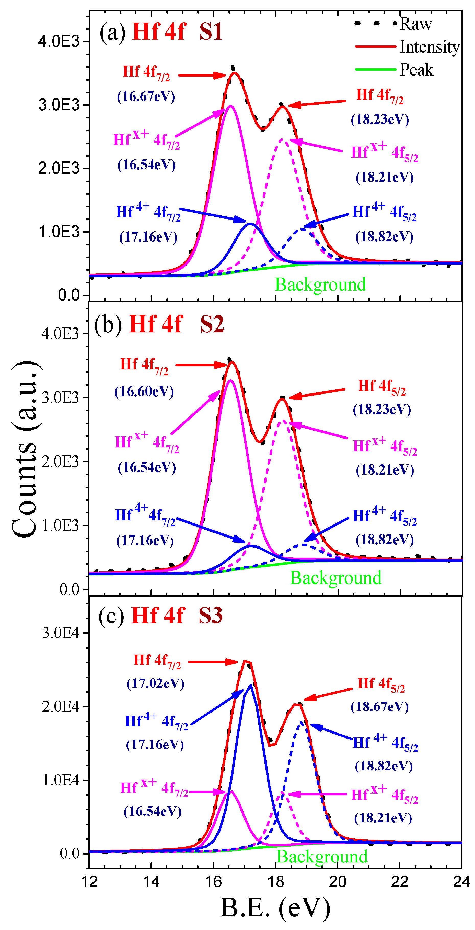
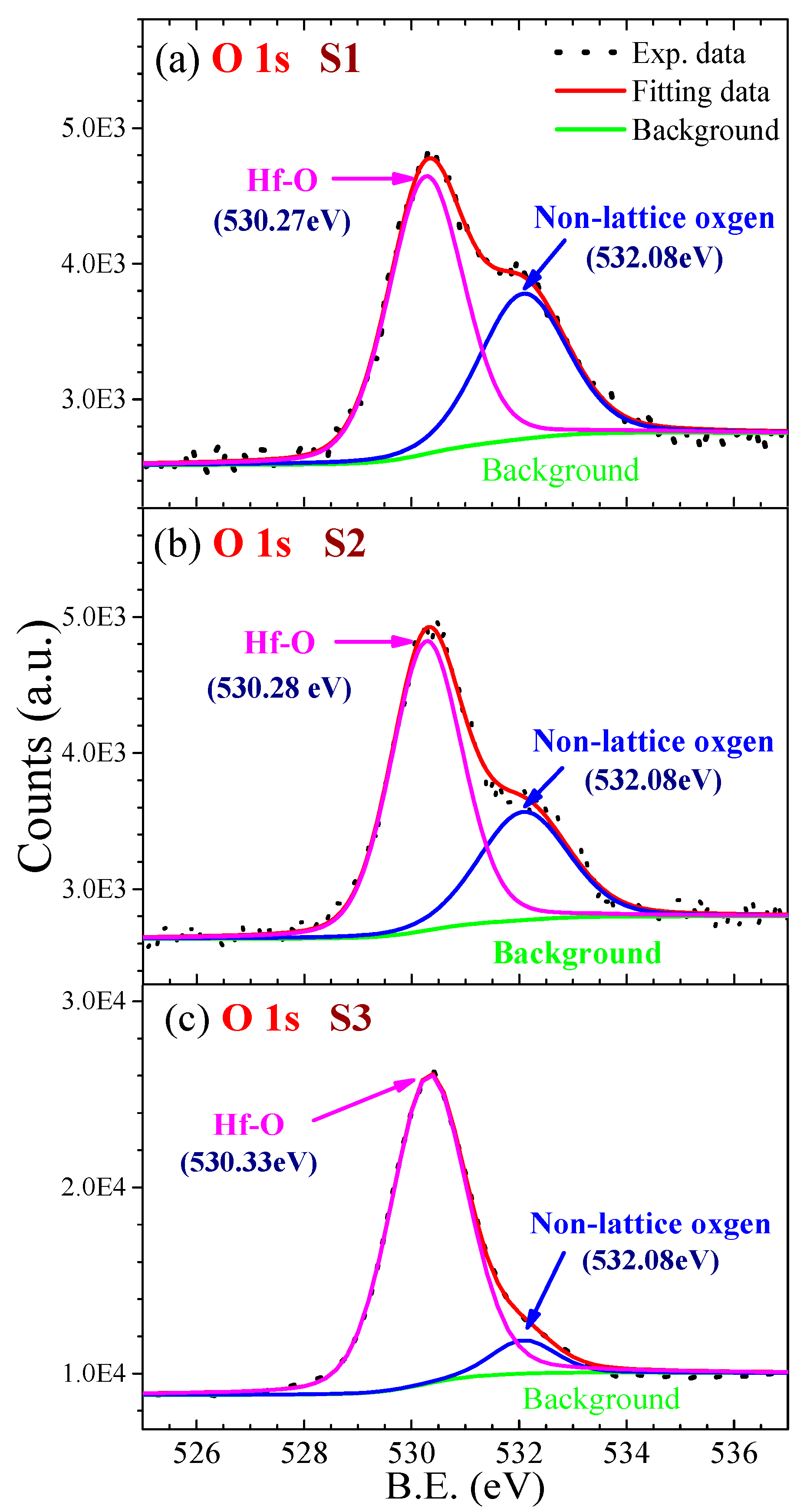
3.1.2. XPS Fitting and the Elements Composition Calculating

High-resolution XPS scans on the Hf 4f and O 1s peaks were performed for three HfO2 films, as shown in Figure 2a–c. We focus on the analyses of the asymmetric shape of the Hf 4f and O 1s spectra to reveal the relative atomic percentage and bonding phase in the surface region. The background subtraction was carried out using Shirley’s iterative method. The baseline of background is a combination of Shirley and linear function. The fitting program XPSPEAK4.1 was used to fit the experimental curves with a Gaussian–Lorenzian mixed function [17]. From the Hf 4f doublet, Hf 4f7/2 and Hf 4f5/2, the spin-orbit splitting and the intensity ratio of the components were set at 1.67 eV and 4/3, respectively [18].
Details of the Hf 4f fine spectra of three samples are shown in Figure 2a–c, respectively. The Hf 4f spectrum could be fitted with two sets of double-peak components. One set at 17.16 eV and 18.83 eV correspond to the Hf4+ 4f7/2 and Hf4+ 4f5/2 peaks of the Hf oxide bond (O–Hf–O), respectively [11]. While another set at 16.50 eV and 18.26 eV correspond to the Hfx+ 4f7/2 and Hfx+ 4f5/2 peaks (x < 4) of the Hf suboxide bond, respectively [19,20]. It is obvious that the doublet peaks of the suboxidized Hfx+ are stronger than those of the fully oxidized Hf4+ from the Figure 2a,b. However, the situation is opposite in Figure 2c. The full width at half maximum (FWHM) of fitted peaks are shown in Table 2. In comparison, the corresponding FWHMs of the Hf4+ in Figure 2a,b are wider than that in Figure 2c. This increased width was caused from the presence of a higher degree of disorder in the deficient films or from the coexistence of tetragonal and monoclinic phases with small differences in binding energy [18]. Our GIXRD data also support this scenario, with discussion in Section 3.3.
A number of factors could lead to the binding energy shifts, such as charge transfer effect, environmental charge density, presence of electric field, and hybridization. Among these factors, charge transfer causing a binding energy shift is regarded as the dominant mechanism for the S2 and S3, with different oxygen flow rates in growth conditions [21]. According to the charge transfer mechanism, an electron removed from the valence orbital generates the increment in core electron’s potential, and finally leads to a chemical binding energy shift [22]. The difference between the sample S2 in Figure 2b and the S3 in Figure 2c is attributed to the difference of the oxygen flow rates. In the deposition process of the S3, Hf oxide bonds were dominate over Hf suboxide bonds, due to the excess oxygen at 800 sccm oxygen flow rate. On the contrary, the sample S2 with 500 sccm oxygen flow rate exhibited a reverse trend: Hf suboxide bonds dominating over Hf oxide bonds. Therefore, it is reasonable that the peaks shift, from 16.60 to 17.02 eV for Hf 4f7/2, and from 18.23 to 18.67 eV for Hf 4f5/2, as shown in Figure 2b,c, can be explained from the enhanced charge transfer with the increase of the O2 gas flow [23]. The intensity change between the Hf4+ 4f and Hfx+ 4f peaks can be demonstrated from the chemical shift in the binding energy of the Hf 4f peaks with oxygen flow rate. Both the Hfx+ 4f7/2 and Hfx+ 4f5/2 peaks in Figure 2a,b have similarly dominated components for the Hf 4f7/2 and Hf 4f5/2 peaks, respectively, while they are weaker than the Hf4+ 4f7/2 and Hf4+ 4f5/2 peaks, respectively in Figure 2c.
In Figure 3a–c, the XPS fitting results on the O 1s peaks of S1, S2, and S3 are shown, respectively. The O 1s peak actually consist of two very closely peaks, the Hf–O bond of O–Hf–O at 530.28~530.40 eV, and the O–O bond of non-lattice oxygen at 532.08 eV, which was contributed to by the suboxides with Hf [17,24,27,28]. The Hf–O bond belongs to the lattice oxygen which dominates in the Figure 2c. This demonstrates that the corresponding samples have ordered structures and good qualities at surface. In the Figure 2a,b, the high percentage of the non-lattice oxygen peak at 532.08 eV from the O 1s spectra indicates more defects existed in the HfO2 film layer surface of S1 and S2.
Comparing the areas of O 1s and Hf 4f peaks, the stoichiometric composition ratio of O and Hf elements at the surface layer of the HfO2 film can be estimated from the XPS fitting results. The atomic percentages and the FWHMs of the XPS O 1s and Hf 4f peaks for HfO2 films deposited on Si are summarized in Table 2. There are some differences among these three samples in their XPS fitting results. The compositions of Hf are 31.63%, 33.10%, and 36.95% for S1, S2 and S3, respectively. The surface ratios of O and Hf elements of the three samples are between 1.70 and 2.13, which are in accordance with the range calculated by Myoung-Seok Kim et al. [23]. The higher proportions of oxygen in the sample of S1 and S2 are due to the presence of the non-lattice oxygen.

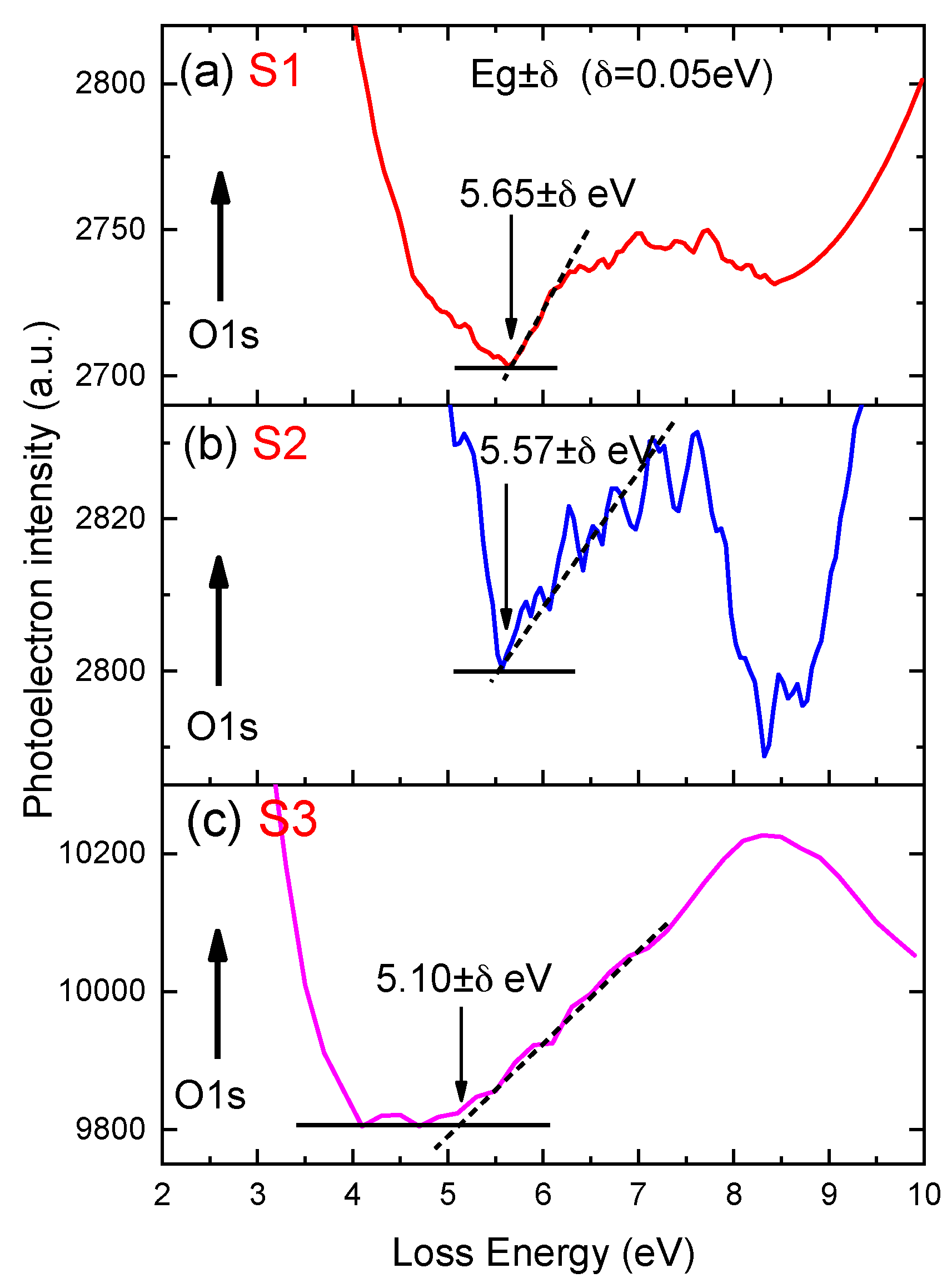
3.1.3. Energy Bandgaps of HfO2 Deduced from XPS

The energy bandgap values of thin oxides can be deduced from the energy loss signals for O 1s photoelectrons [25,26]. The photoelectron loss-energy spectra of three HfO2 films are shown in Figure 4. The start of the photoelectron loss-energy spectrum, after setting the energy of the O 1s peak maximum to zero loss energy, was defined by linearly extrapolating the segment of maximum negative slope (dash-lines in the Figure 4) to the background level in each of the spectra [29,30,31]. The bandgap values of S1, S2, and S3 are as follows: 5.65 eV, 5.57 eV and 5.10 eV, which are in agreement with our results by variable angle spectroscopic ellipsometry (VASE) in Section 3.4, and previously reported bandgap values for HfO2 in different references [3,32,33,34,35,36,37].

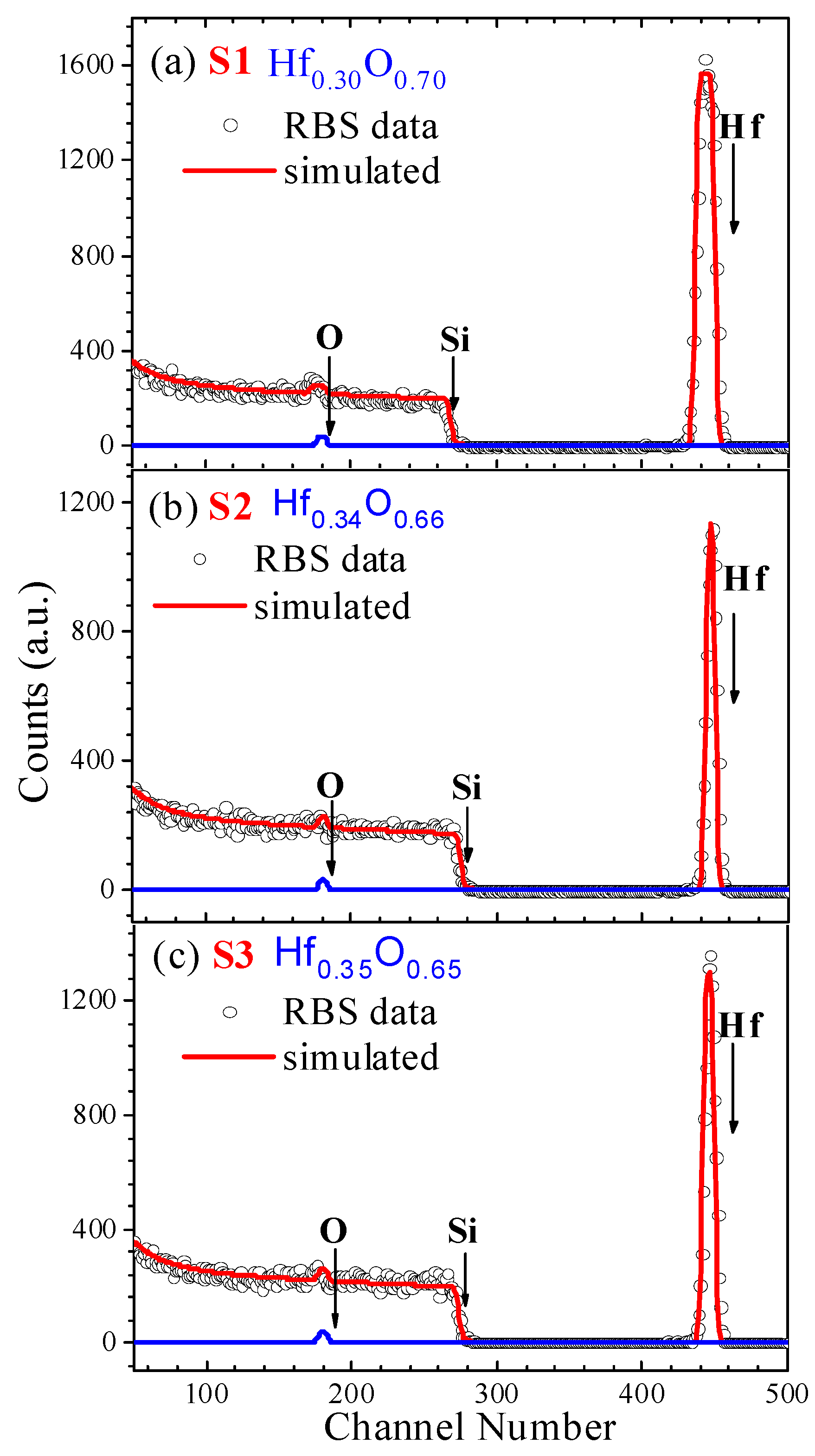
3.2. Rutherford Backscattering Spectrometry (RBS)

The random RBS spectra for three HfO2 layers on Si and their corresponding simulated fits by SIMNRA are given in Figure 5. The contents of three HfO2 films are determined precisely and listed in Table 3, and the calculated film thicknesses are shown in Table 5. The arrows (labeled with Hf, O, and Si) in Figure 5 denote the energy for backscattering from Hf, O, and Si atoms, respectively. The perfectly symmetrical shapes of the hafnium peaks indicate a negligible film roughness of the three samples with respect to the mean thickness [38].
Although the RBS probes the entire film and the XPS mainly the surface area of only about 5–10 nm, they are particularly close to the expected ideal composition value of Hf0.33O0.67. The measurements of XPS and RBS suggest that the stoichiometric HfO2 films were deposited dominantly on Si. However, there is still a little deviation between the simulated compositions by RBS and XPS for all samples. For the S1 and S2 films, from both RBS and XPS, the ratios (Hf:O) are 1:N (N > 2). There exists a bit over stoichiometry oxygen, which might be caused from the non-lattice oxygen, as discussed in Section 3.1.2. For the film S3, the ratios (Hf:O) from both RBS and XPS are 1:N (N < 2), indicating a small over stoichiometry hafnium, which might be attributed from the sub-oxidized Hfx+ (x < 4), such as the theoretically predicted semi-metallic Hf2O3 [9,39].

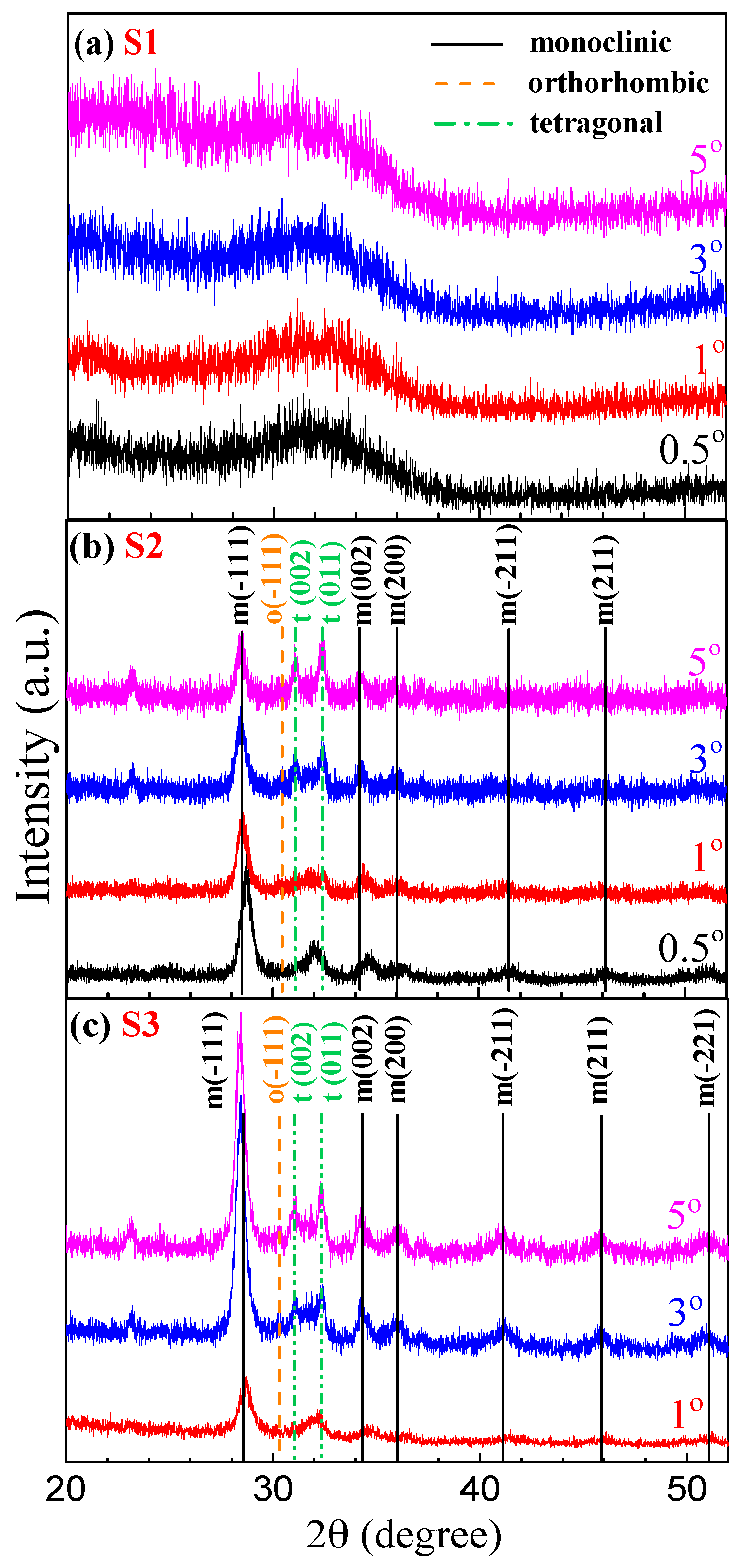
3.3. Grazing Incidence X-ray Diffraction (GIXRD)

Grazing incidence X-ray diffraction (GIXRD) patterns of S1, S2, and S3 with different incident angles (0.5°, 1°, 3°, and 5°) are shown in Figure 6, respectively. These spectra demonstrate the crystallization and the crystallization phases of the thin HfO2 films, and variations from the surface to the interface corresponding to the incident angle from 0.5° to 5°. The broad GIXRD curves in Figure 6a indicate that the HfO2 film of S1 is amorphous in nature. This is due to the fact that the low deposition temperature of 400 °C cannot provide sufficient energy to form a crystalline HfO2 layer by AVD [40,41,42]. The GIXRD patterns of samples S2 and S3 deposited at substrate temperature of 500 °C indicate that these HfO2 films are polycrystalline. The peaks of GIXRD patterns in Figure 6b,c are indexed by the monoclinic, tetragonal, and orthorhombic phases, correspondingly. It is noted that orientation indexes of (−111), (002), (200), (−211), (211), and (−221) correspond to the dominant monoclinic phase of HfO2 film. The low intensity peak at 2θ = 30.5° refers to the (−111) orthorhombic phases [43,44]. There are two peaks at 31.0° and 32.3°, being attributed to the (002) tetragonal and (011) tetragonal phases of Hf2O3, respectively, according to the calculated data by Kan-Hao Xue et al. [39].
In the Figure 6b,c, the peaks of monoclinic, tetragonal, and orthorhombic phases are clearly seen at 3° and 5° incidences. When the detection angles were at 1° and 0.5°, the m(−111) peaks of monoclinic phase are dominant, and the peaks of orthorhombic and tetragonal phase are weak to hardly visible. In other words, there are three phases deposited at the initial stage of film growth. As the thickness increases, the tetragonal and orthorhombic phases gradually weaken to almost invisible. Recently, it was reported that HfO2 thin films could be crystallized in both orthorhombic and tetragonal phases when they are sufficiently thin (<10 nm) and the grain size is small [45,46]. Our investigation revealed that the HfO2 layer had all monoclinic, tetragonal, and orthorhombic structural phases at its initial growth stage, but as they grow thicker, the tetragonal and orthorhombic phases become weaker, and finally almost disappeared.
By the Scherrer formula, the crystallite size of HfO2 thin film of S2 and S3 with different incident angles can be calculated using the m(−111) peak of the monoclinic phase [47,48,49].
D = k · λ β cos θ ,
where D is the crystallite size, λ is the X-ray wavelength of Cu (0.15418 nm), k is the Scherrer constant of the order of unity (0.95 for powder and 0.89 for film), β is the full width of peak at half maximum intensity (FWHM), and θ is the corresponding Bragg diffraction angle [47,48,49].
Figure 7 exhibits the m(−111) peak patterns of monoclinic phase of S2 and S3 with incident angles of 0.5°, 1°, 3° and 5°, from Figure 6b,c, respectively. The values of the peak position, FWHM and the calculated crystallite size are listed in Table 4. As the incident angle varies from 5° to 0.5°, i.e., decreasing the depth of detection, the m(−111) peak positions were shifted towards the high angle side and their FWHMs were increased, both gradually. Also, the crystallite size became smaller with decreasing the depth of detection. Generally, the crystal lattice with dwindling crystal size tends to generate phases of higher symmetry [50,51]. These correspond to the appearance of tetragonal and orthorhombic phases in Figure 6b,c. Multiple mixed crystal phases result in the lower symmetry of the HfO2 in the depths.
In Table 4, the relatively similar data on the crystallite size (D) for S2 and S3 show that there is no obvious difference in microcosmic. However, the sharp and intense peaks of S3 in the XRD spectra, shown in Figure 6 and Figure 7, demonstrate its structure is more orderly than S2 on a large scale. Among the GIXRD patterns of S1, S2 and S3, the structure of S3 is the most orderly, and its quality is the best among these three samples, which are consistent with our results from XPS and RBS measurements and analyses.

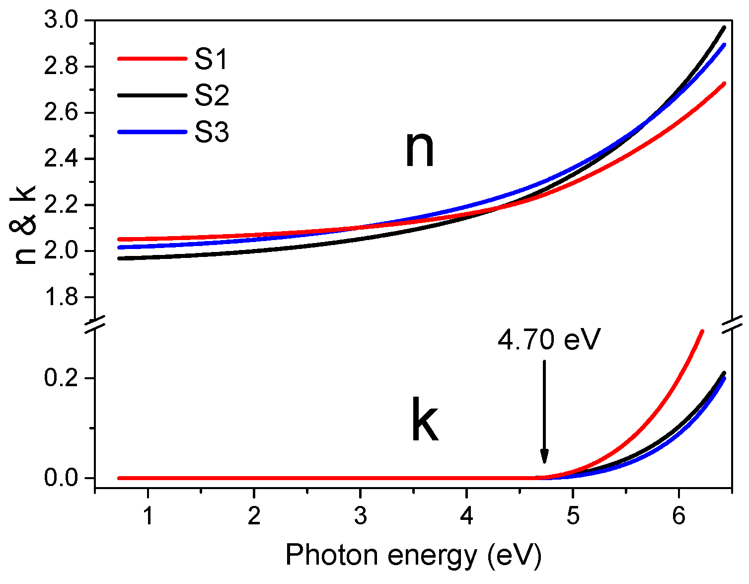
3.4. The Variable Angle Spectroscopic Ellipsometry (VASE)

The best fit results of VASE spectra for HfO2/Si sample S3 are presented in Figure 8, where dot lines depict SE experiment data, and solid lines are the fitting results. The data displayed for two key ellipsometry parameters, Psi (Ψ) and Delta (Δ), are related to the change in amplitude and phase shift of the impinging E field upon reflection, and are wavelength dependent [52]. In our analyses, we have considered an interface region with silicate (SiOx), which is observed clearly in the interface by high-resolution transmission electron microscope (HR-TEM), as shown in Figure 9. The surface roughness was described by Bruggeman effective medium approximation (EMA) [52,53]. The fitting structural model were constructed as silicon substrate/interface layer/HfO2 layer/surface roughness. In order to get more reliable fitting results, the VASE spectra were measured with five incident angles of 50°, 55°, 60°, 65°, and 70°for the three samples. The fitted thicknesses of roughness, HfO2 layer, and interface layer for three samples were obtained from VASE.
In Table 5, the thicknesses of the corresponding layer of S1, S2 and S3 are close from different measurements, including VASE, RBS, HR-TEM, and the measured thicknesses from the grower. It is more accurate about the thicknesses from HR-TEM and VASE. In comparison with the interface thicknesses of three samples, higher substrate temperatures, and larger oxygen flow in growth progress result in thicker interface of silicate.
The fitted optical constants of refractive index n and extinction coefficient k are presented in Figure 10. As the photon energy is less than 4.70 eV, the HfO2 films are at the transparent region. However, the extinction coefficients start to increase rapidly at the high-energy edge from 4.70 eV, resulting from the remarkable subgap absorption [16].
The HfO2 films are known to have an indirect bandgap. Its optical bandgap versus photon energy is proportional to (αhν)1/2, ((αhν)2 for direct bandgap material), where α and are the absorption coefficient and photon energy, respectively [3,14,54,55,56]. Figure 11 shows plots of (αhν)1/2 versus photon energy for our three HfO2 films, respectively. The values of the optical bandgap Eg were calculated by the liners of (αhν)1/2 vs. extrapolated to the intersection with the photon energy axis. The bandgaps of HfO2 films of S1, S2 and S3 were determined to be 5.35 eV, 5.34 eV, and 5.26 eV, respectively. These data are approximate to the values of bandgap obtained from the photoelectron energy-loss spectra by XPS in Section 3.1. Associated with the analysis results of GIXRD, the better quality of samples are related to the smaller bandgaps.

4. Conclusions

Comprehensive analyses have been conducted on a series of HfO2 thin (30–70 nm) films grown on Si by AVD under different growth conditions via XPS, RBS, GIXRD, and VASE. The film characteristic parameters of thickness, structures, optical constants, bandgaps etc. were accurately determined. Important and significant results are obtained:
  • Through XPS measurements and analyses on the Hf 4f peaks and the change of intensity ratio between Hf4+ and Hfx+ peaks, it was revealed that at the lower oxygen flow rate of 500 sccm, the insufficient chemical reaction leaded to more Hf suboxide bonds and non-lattice oxygen produced at HfO2 film surface; while, as the oxygen flow rate increased to 800 sccm, the quality of the surface films had been significantly improved.
  • The deposited HfO2 films on Si were amorphous in nature at the low deposition temperature of 400 °C by AVD, while at higher deposition temperature, polycrystalline HfO2 films were achieved.
  • At the initial stage of film growth, the monoclinic, tetragonal, and orthorhombic phases co-existed. As the film grew thicker, the tetragonal and orthorhombic phases gradually weakened until the monoclinic phase dominated. The crystallite size of HfO2 film became smaller from interface to surface, confirmed using varied angle GIXRD.
  • It was found that for HfO2 film, higher crystallization and more ordered structure correspond to a smaller bandgap, determined from VASE and XPS, close to single crystal HfO2.
The comprehensive studies demonstrate that appropriate substrate temperature and oxygen flow are essential to the structure, chemical composition, and optical constants from surface and interface of the HfO2 films deposited by AVD. This work with integrated experiment measurements and analyses has enhanced our understanding of AVD-grown HfO2 advanced materials.

Author Contributions

Conceptualization, X.L., X.L., L.W. and Z.C.F.; Data curation, X.L.; Formal analysis, X.L., Y.L. and H.Y.; Funding acquisition, L.W. and W.S.; Investigation, X.L. and Y.L.; Project administration, Z.C.F.; Resources, H.-H.L., S.Y. and Z.C.F.; Supervision, Z.C.F.; Writing—original draft, X.L.; Writing—review & editing, X.L., Y.L., H.Y., Y.L., L.W., W.S., K.H. and Z.C.F.

Acknowledgments

This work was supported by the National Natural Science Foundation of China [Nos. 61367004 and 61504030]; and the special funding [Nos. T3120097921 and T3120099202] for Guangxi distinguished [Bagui Rencai & Bagui Xuezhe].

Conflicts of Interest

The authors declare no conflict of interest.

References

  1. Lu, Q.; Huang, R.; Lan, X.; Chi, X.; Lu, C.; Li, C.; Wu, Z.; Li, J.; Han, G.; Yan, P. Amazing diffusion depth of ultra-thin hafnium oxide film grown on n-type silicon by lower temperature atomic layer deposition. Mater. Lett. 2016, 169, 164–167. [Google Scholar] [CrossRef]
  2. Gao, L.; Yalon, E.; Chew, A.R.; Deshmukh, S.; Salleo, A.; Pop, E.; Demkov, A.A. Effect of oxygen vacancies and strain on the phonon spectrum of HfO2 thin films. J. Appl. Phys. 2017, 121, 224101. [Google Scholar] [CrossRef]
  3. Fan, X.; Liu, H.; Zhong, B.; Fei, C.; Wang, X.; Wang, Q. Optical characteristics of H2O-based and O3-based HfO2 films deposited by ALD using spectroscopy ellipsometry. Appl. Phys. A 2015, 119, 957–963. [Google Scholar] [CrossRef]
  4. Shandalov, M.; McIntyre, P.C. Size-dependent polymorphism in HfO2 nanotubes and nanoscale thin films. J. Appl. Phys. 2009, 106, 084322. [Google Scholar] [CrossRef]
  5. Kim, J.C.; Heo, J.S.; Cho, Y.S.; Moon, S.H. Atomic layer deposition of an HfO2 thin film using Hf(O-iPr)4. Thin Solid Films 2009, 517, 5695–5699. [Google Scholar] [CrossRef]
  6. Monaghan, S.; Hurley, P.K.; Cherkaoui, K.; Negara, M.A.; Schenk, A. Determination of electron effective mass and electron affinity in HfO2 using MOS and MOSFET structures. Solid-State Electron. 2009, 53, 438–444. [Google Scholar] [CrossRef]
  7. Cosnier, V.; Dabertrand, K.; Blonkowski, S.; Lhostis, S.; Zoll, S.; Morand, Y.; Descombes, S.; Guillaumot, B.; Hobbs, C.; Rochat, N.; et al. Atomic Vapour Deposition (AVD™) Process for High Performance HfO2 Dielectric Layers. MRS Proc. 2004, 811, 287–292. [Google Scholar] [CrossRef]
  8. Schumacher, M.; Baumann, P.K.; Seidel, T. AVD and ALD as Two Complementary Technology Solutions for Next Generation Dielectric and Conductive Thin-Film Processing. Chem. Vapor Depos. 2006, 12, 99–108. [Google Scholar] [CrossRef]
  9. Leu, C.-C.; Lin, C.-H.; Chien, C.-H.; Yang, M.-J. Effects of HfO2 buffer layer thickness on the properties of Pt/SrBi2Ta2O9/HfO2/Si structure. J. Mater. Res. 2008, 23, 2023–2032. [Google Scholar] [CrossRef]
  10. Lin, C.-P.; Tsui, B.-Y.; Yang, M.-J.; Huang, R.-H.; Chien, C.-H. High-performance poly-silicon TFTs using HfO2 gate dielectric. IEEE Electron Device Lett. 2006, 27, 360–363. [Google Scholar] [CrossRef]
  11. Manikanthababu, N.; Dhanunjaya, M.; Nageswara Rao, S.V.S.; Pathak, A.P. SHI induced effects on the electrical and optical properties of HfO2 thin films deposited by RF sputtering. Nucl. Instrum. Methods Phys. Res. Sect. B Beam Interact. Mater. Atoms 2016, 379, 230–234. [Google Scholar] [CrossRef]
  12. He, G.; Jiang, S.; Li, W.; Zheng, C.; He, H.; Li, J.; Sun, Z.; Liu, Y.; Liu, M. Interface chemistry and electronic structure of ALD-derived HfAlO/Ge gate stacks revealed by X-ray photoelectron spectroscopy. J. Alloys Compd. 2017, 716, 1–6. [Google Scholar] [CrossRef]
  13. Cho, Y.J.; Nguyen, N.V.; Richter, C.A.; Ehrstein, J.R.; Lee, B.H.; Lee, J.C. Spectroscopic ellipsometry characterization of high-k dielectric HfO2 thin films and the high-temperature annealing effects on their optical properties. Appl. Phys. Lett. 2002, 80, 1249–1251. [Google Scholar] [CrossRef]
  14. Takeuchi, H.; Ha, D.; King, T.-J. Observation of bulk HfO2 defects by spectroscopic ellipsometry. J. Vac. Sci. Technol. A Vac. Surf. Films 2004, 22, 1337–1341. [Google Scholar] [CrossRef]
  15. Buiu, O.; Lu, Y.; Mitrovic, I.Z.; Hall, S.; Chalker, P.; Potter, R.J. Spectroellipsometric assessment of HfO2 thin films. Thin Solid Films 2006, 515, 623–626. [Google Scholar] [CrossRef]
  16. Sancho-Parramon, J.; Modreanu, M.; Bosch, S.; Stchakovsky, M. Optical characterization of HfO2 by spectroscopic ellipsometry: Dispersion models and direct data inversion. Thin Solid Films 2008, 516, 7990–7995. [Google Scholar] [CrossRef]
  17. Pang, H.; Deng, N. A Forming-Free Bipolar Resistive Switching in HfOx -Based Memory with a Thin Ti Cap. Chin. Phys. Lett. 2014, 31, 107303. [Google Scholar] [CrossRef]
  18. Sharath, S.U.; Bertaud, T.; Kurian, J.; Hildebrandt, E.; Walczyk, C.; Calka, P.; Zaumseil, P.; Sowinska, M.; Walczyk, D.; Gloskovskii, A.; et al. Towards forming-free resistive switching in oxygen engineered HfO2−x. Appl. Phys. Lett. 2014, 104, 063502. [Google Scholar] [CrossRef]
  19. Tan, T.; Guo, T.; Wu, Z.; Liu, Z. Charge transport and bipolar switching mechanism in a Cu/HfO2/Pt resistive switching cell. Chin. Phys. B 2016, 25, 117306. [Google Scholar] [CrossRef]
  20. Zhang, W.; Kong, J.-Z.; Cao, Z.-Y.; Li, A.-D.; Wang, L.-G.; Zhu, L.; Li, X.; Cao, Y.-Q.; Wu, D. Bipolar Resistive Switching Characteristics of HfO2/TiO2/HfO2 Trilayer-Structure RRAM Devices on Pt and TiN-Coated Substrates Fabricated by Atomic Layer Deposition. Nanoscale Res. Lett. 2017, 12. [Google Scholar] [CrossRef] [PubMed]
  21. Kondaiah, P.; Shaik, H.; Mohan Rao, G. Studies on RF magnetron sputtered HfO2 thin films for microelectronic applications. Electron. Mater. Lett. 2015, 11, 592–600. [Google Scholar] [CrossRef]
  22. Bagus, P.S.; Illas, F.; Pacchioni, G.; Parmigiani, F. Mechanisms responsible for chemical shifts of core-level binding energies and their relationship to chemical bonding. J. Electron Spectrosc. Relat. Phenom. 1999, 100, 215–236. [Google Scholar] [CrossRef]
  23. Kim, M.-S.; Ko, Y.-D.; Yun, M.; Hong, J.-H.; Jeong, M.-C.; Myoung, J.-M.; Yun, I. Characterization and process effects of HfO2 thin films grown by metal-organic molecular beam epitaxy. Mater. Sci. Eng. B 2005, 123, 20–30. [Google Scholar] [CrossRef]
  24. Guo, T.; Tan, T.; Liu, Z. Resistive switching behavior of HfO2 film with different Ti doping concentrations. J. Phys. D Appl. Phys. 2016, 49, 045103. [Google Scholar] [CrossRef]
  25. Miyazaki, S.; Narasaki, M.; Ogasawara, M.; Hirose, M. Characterization of ultrathin zirconium oxide films on silicon using photoelectron spectroscopy. Microelectron. Eng. 2001, 59, 373–378. [Google Scholar] [CrossRef]
  26. David, D.; Godet, C. Derivation of dielectric function and inelastic mean free path from photoelectron energy-loss spectra of amorphous carbon surfaces. Appl. Surf. Sci. 2016, 387, 1125–1139. [Google Scholar] [CrossRef] [Green Version]
  27. Mondal, S.; Chen, H.-Y.; Her, J.-L.; Ko, F.-H.; Pan, T.-M. Effect of Ti doping concentration on resistive switching behaviors of Yb2O3 memory cell. Appl. Phys. Lett. 2012, 101, 083506. [Google Scholar] [CrossRef]
  28. Lee, M.J.; Park, Y.; Ahn, S.E.; Kang, B.S.; Lee, C.B.; Kim, K.H.; Xianyu, W.X.; Yoo, I.K.; Lee, J.H.; Chung, S.J.; et al. Comparative structural and electrical analysis of NiO and Ti doped NiO as materials for resistance random access memory. J. Appl. Phys. 2008, 103, 013706. [Google Scholar] [CrossRef] [Green Version]
  29. Tang, T.; Zhang, Z.M.; Ding, Z.J.; Yoshikawa, H. Deriving Effective Energy Loss Function for Silver from XPS Spectrum. Phys. Procedia 2012, 32, 165–172. [Google Scholar] [CrossRef]
  30. Miyazaki, S. Photoemission study of energy-band alignments and gap-state density distributions for high-k gate dielectrics. J. Vac. Sci. Technol. B Microelectron. Nanometer Struct. 2001, 19, 2212. [Google Scholar] [CrossRef]
  31. Miyazaki, S.; Narasaki, M.; Ogasawara, M.; Hirose, M. Chemical and electronic structure of ultrathin zirconium oxide films on silicon as determined by photoelectron spectroscopy. Solid-State Electron. 2002, 46, 1679–1685. [Google Scholar] [CrossRef]
  32. Xu, D.-P.; Yu, L.-J.; Chen, X.-D.; Chen, L.; Sun, Q.-Q.; Zhu, H.; Lu, H.-L.; Zhou, P.; Ding, S.-J.; Zhang, D.W. In Situ Analysis of Oxygen Vacancies and Band Alignment in HfO2/TiN Structure for CMOS Applications. Nanoscale Res. Lett. 2017, 12, 311. [Google Scholar] [CrossRef] [PubMed]
  33. Huang, M.L.; Chang, Y.C.; Chang, Y.H.; Lin, T.D.; Kwo, J.; Hong, M. Energy-band parameters of atomic layer deposited Al2O3 and HfO2 on InxGa1−xAs. Appl. Phys. Lett. 2009, 94, 052106. [Google Scholar] [CrossRef]
  34. Gaumer, C.; Martinez, E.; Lhostis, S.; Guittet, M.-J.; Gros-Jean, M.; Barnes, J.-P.; Licitra, C.; Rochat, N.; Barrett, N.; Bertin, F.; et al. Impact of the TiN electrode deposition on the HfO2 band gap for advanced MOSFET gate stacks. Microelectron. Eng. 2011, 88, 72–75. [Google Scholar] [CrossRef]
  35. Martínez, F.L.; Toledano-Luque, M.; Gandía, J.J.; Cárabe, J.; Bohne, W.; Röhrich, J.; Strub, E.; Mártil, I. Optical properties and structure of HfO2 thin films grown by high pressure reactive sputtering. J. Phys. D Appl. Phys. 2007, 40, 5256–5265. [Google Scholar] [CrossRef]
  36. Cantas, A.; Aygun, G.; Basa, D.K. In-situ spectroscopic ellipsometry and structural study of HfO2 thin films deposited by radio frequency magnetron sputtering. J. Appl. Phys. 2014, 116, 083517. [Google Scholar] [CrossRef]
  37. Vargas, M.; Murphy, N.R.; Ramana, C.V. Structure and optical properties of nanocrystalline hafnium oxide thin films. Opt. Mater. 2014, 37, 621–628. [Google Scholar] [CrossRef]
  38. Blanchin, M.-G.; Canut, B.; Lambert, Y.; Teodorescu, V.S.; Barău, A.; Zaharescu, M. Structure and dielectric properties of HfO2 films prepared by a sol-gel route. J. Sol-Gel Sci. Technol. 2008, 47, 165–172. [Google Scholar] [CrossRef]
  39. Xue, K.-H.; Blaise, P.; Fonseca, L.R.C.; Nishi, Y. Prediction of Semimetallic Tetragonal Hf2O3 and Zr2O3 from First Principles. Phys. Rev. Lett. 2013, 110, 065502. [Google Scholar] [CrossRef] [PubMed]
  40. Martin, N.; Rousselot, C.; Rondot, D.; Palmino, F.; Mercier, R. Microstructure modification of amorphous titanium oxide thin films during annealing treatment. Thin Solid Films 1997, 300, 113–121. [Google Scholar] [CrossRef]
  41. Aguirre, B.; Vemuri, R.S.; Zubia, D.; Engelhard, M.H.; Shutthananadan, V.; Bharathi, K.K.; Ramana, C.V. Growth, microstructure and electrical properties of sputter-deposited hafnium oxide (HfO2) thin films grown using a HfO2 ceramic target. Appl. Surf. Sci. 2011, 257, 2197–2202. [Google Scholar] [CrossRef]
  42. Ramzan, M.; Rana, A.M.; Ahmed, E.; Wasiq, M.F.; Bhatti, A.S.; Hafeez, M.; Ali, A.; Nadeem, M.Y. Optical characterization of hafnium oxide thin films for heat mirrors. Mater. Sci. Semicond. Process. 2015, 32, 22–30. [Google Scholar] [CrossRef]
  43. Pal, A.; Narasimhan, V.K.; Weeks, S.; Littau, K.; Pramanik, D.; Chiang, T. Enhancing ferroelectricity in dopant-free hafnium oxide. Appl. Phys. Lett. 2017, 110, 022903. [Google Scholar] [CrossRef]
  44. Polakowski, P.; Müller, J. Ferroelectricity in undoped hafnium oxide. Appl. Phys. Lett. 2015, 106, 232905. [Google Scholar] [CrossRef]
  45. Park, M.H.; Lee, Y.H.; Kim, H.J.; Kim, Y.J.; Moon, T.; Kim, K.D.; Müller, J.; Kersch, A.; Schroeder, U.; Mikolajick, T.; et al. Ferroelectricity and Antiferroelectricity of Doped Thin HfO2 -Based Films. Adv. Mater. 2015, 27, 1811–1831. [Google Scholar] [CrossRef] [PubMed]
  46. Kim, K.D.; Park, M.H.; Kim, H.J.; Kim, Y.J.; Moon, T.; Lee, Y.H.; Hyun, S.D.; Gwon, T.; Hwang, C.S. Ferroelectricity in undoped-HfO2 thin films induced by deposition temperature control during atomic layer deposition. J. Mater. Chem. C 2016, 4, 6864–6872. [Google Scholar] [CrossRef]
  47. Fu, W.-E.; Chang, Y.-Q.; Chen, Y.-C.; Secula, E.M.; Seiler, D.G.; Khosla, R.P.; Herr, D.; Michael Garner, C.; McDonald, R.; Diebold, A.C. Post-deposition annealing analysis for HfO2 thin films using GIXRR/GIXRD. In AIP Conference Proceedings; American Institute of Physics: College Park, MD, USA, 2009; Volume 1173, pp. 122–126. [Google Scholar]
  48. Pandey, S.; Kothari, P.; Sharma, S.K.; Verma, S.; Rangra, K.J. Impact of post deposition annealing in O2 ambient on structural properties of nanocrystalline hafnium oxide thin film. J. Mater. Sci. Mater. Electron. 2016, 27, 7055–7061. [Google Scholar] [CrossRef]
  49. Ramadoss, A.; Krishnamoorthy, K.; Kim, S.J. Facile synthesis of hafnium oxide nanoparticles via precipitation method. Mater. Lett. 2012, 75, 215–217. [Google Scholar] [CrossRef]
  50. Ayyub, P.; Palkar, V.R.; Chattopadhyay, S.; Multani, M. Effect of crystal size reduction on lattice symmetry and cooperative properties. Phys. Rev. B 1995, 51, 6135–6138. [Google Scholar] [CrossRef]
  51. Matovic, B.; Pantic, J.; Lukovic, J.; Cebela, M.; Dmitrovic, S.; Mirkovic, M.; Prekajski, M. A novel reduction–oxidation synthetic route for hafnia. Ceram. Int. 2016, 42, 615–620. [Google Scholar] [CrossRef]
  52. Chen, S.; Li, Q.; Ferguson, I.; Lin, T.; Wan, L.; Feng, Z.C.; Zhu, L.; Ye, Z. Spectroscopic ellipsometry studies on ZnCdO thin films with different Cd concentrations grown by pulsed laser deposition. Appl. Surf. Sci. 2017, 421, 383–388. [Google Scholar] [CrossRef]
  53. Liu, Y.; Li, Q.X.; Wan, L.Y.; Kucukgok, B.; Ghafari, E.; Ferguson, I.T.; Zhang, X.; Wang, S.; Feng, Z.C.; Lu, N. Composition and temperature dependent optical properties of AlxGa1-x N alloy by spectroscopic ellipsometry. Appl. Surf. Sci. 2017, 421, 389–396. [Google Scholar] [CrossRef]
  54. Ding, L.; Friedrich, M.; Fronk, M.; Gordan, O.D.; Zahn, D.R.T.; Chen, L.; Wei Zhang, D.; Cobet, C.; Esser, N. Correlation of band gap position with composition in high-k films. J. Vac. Sci. Technol. B Nanotechnol. Microelectron. Mater. Process. Meas. Phenom. 2014, 32, 03D115. [Google Scholar] [CrossRef]
  55. Di, M.; Bersch, E.; Diebold, A.C.; Consiglio, S.; Clark, R.D.; Leusink, G.J.; Kaack, T. Comparison of methods to determine bandgaps of ultrathin HfO2 films using spectroscopic ellipsometry. J. Vac. Sci. Technol. A Vac. Surf. Films 2011, 29, 041001. [Google Scholar] [CrossRef]
  56. Park, J.-W.; Lee, D.-K.; Lim, D.; Lee, H.; Choi, S.-H. Optical properties of thermally annealed hafnium oxide and their correlation with structural change. J. Appl. Phys. 2008, 104, 033521. [Google Scholar] [CrossRef]
Figure 1. XPS survey scan of the HfO2 film of the sample S3.
Crystals 08 00248 g001
Figure 2. The high-resolution XPS fitting results of the Hf 4f peaks of S1, S2, and S3 are shown in (ac), respectively, with experiment data (short dash lines), fitting result (red solid lines) and background (chartreuse solid lines).
Crystals 08 00248 g002
Figure 3. The high-resolution XPS fitting results of the O 1s peaks of S1, S2, and S3 are shown in (ac), respectively, with experiment data (short dash lines), fitting result (red solid lines), and background (chartreuse solid lines).
Crystals 08 00248 g003
Figure 4. The photoelectron energy-loss spectra from the O 1s peaks of HfO2 films for S1, S2 and S3 by XPS are shown in (ac), respectively.
Crystals 08 00248 g004
Figure 5. Random (open circles) and simulated fitting (solid lines) RBS spectra of of S1, S2 and S3 are shown in (ac), respectively.
Crystals 08 00248 g005
Figure 6. Grazing incidence X-ray diffraction (GIXRD) patterns of S1, S2 and S3 with different incident angles (0.5°, 1°, 3° and 5°) are shown in (ac), respectively.
Crystals 08 00248 g006
Figure 7. The m(−111) peak of monoclinic phase of S2 and S3 in GIXRD patterns.
Crystals 08 00248 g007
Figure 8. SE spectra (dot lines) and fitted (solid lines) psi and delta spectra vs photon energy with five incident angles (50°, 55°, 60°, 65° and 70°) of HfO2/Si sample S3 at RT (300 K).
Crystals 08 00248 g008
Figure 9. HR-TEM images of the S3 with scale of (a) 2 nm, and (b) 10 nm, respectively.
Crystals 08 00248 g009
Figure 10. Optical constants of refractive indices (n) and extinction coefficients (k) for three HfO2 films of S1, S2, and S3 at RT (300 K).
Crystals 08 00248 g010
Figure 11. (αhν)1/2 versus photon energy plots of the HfO2 films.
Crystals 08 00248 g011
Table 1. Growth conditions and measured thicknesses of HfO2 thin films by TEM, from the grower.
SampleStructureGrowth ConditionsThicknesses
S1 (Hf08a)HfO2/Si400 °C, 5 mbar, O2: 500 sccm70 nm
S2 (Hf08b)HfO2/Si500 °C, 5 mbar, O2: 500 sccm33 nm
S3 (Hf08c)HfO2/Si500 °C, 5 mbar, O2: 800 sccm34 nm
Table 2. The Hf and O atomic percentages and bonding analyses of S1, S2 and S3.
Sample Hfx+ 4f7/2Hfx+ 4f5/2Hf4+ 4f7/2Hf4+ 4f5/2 OO–Hf
S1Peak/eV16.5418.2117.1618.82Peak/eV532.08530.27
FWHM1.341.321.271.25FWHM1.931.65
Area/ASF
(2.05)
4118.463088.841083.73812.80Area/ASF
(0.66)
2400.193935.01
Atom0.140.110.040.03Atom0.260.42
Hf (%)31.63%O (%)68.37%
S2Peak/eV16.5418.2117.1618.82Peak/eV532.08530.28
FWHM1.281.271.451.39FWHM1.961.57
Area/ASF
(2.05)
4425.813319.36565.70424.27Area/ASF
(0.66)
1822.133885.52
Atom0.170.130.020.02Atom0.210.46
Hf (%)33.01%O (%)66.99%
S3Peak/eV16.5418.2117.1618.82Peak/eV532.08530.33
FWHM0.970.801.061.06FWHM1.381.67
Area/ASF
(2.05)
9172.996879.7427,466.5620,599.92Area/ASF
(0.66)
2901.0132,328.96
Atom0.050.040.160.12Atom0.050.58
Hf (%)36.95%O (%)63.05%
Table 3. The compositions of the three HfO2 films on Si obtained by RBS and XPS.
SamplesHf (Composition)O (Composition)Ratios (Hf:O)
RBSXPSRBSXPSRBSXPS
S1 (Hf08a)0.300.320.700.681:2.331:2.13
S2 (Hf08b)0.340.330.660.671:1.941:2.03
S3 (Hf08c)0.350.370.650.631:1.861:1.70
Table 4. Peak position (2θ (degree)), FWHM (β (degree)), and crystallite size (D (nm)). The average errors estimations are 0.004°, 0.007°, and 0.008 nm, respectively.
Incident AnglesS2S3
(Degree)2θ (Degree)β (Degree)D (nm)2θ (Degree)β (Degree)D (nm)
0.5°28.7200.54814.810
28.5210.52115.57028.6800.60513.413
28.4600.51315.81128.4440.47916.932
28.4490.46017.63228.4260.47217.183
Table 5. The thicknesses of three samples are obtained by VASE, RBS, HR-TEM, and the measured thicknesses from grower.
Thickness (nm)
SamplesSERBSHR-TEMGrower
RoughnessHfO2InterfaceHfO2HfO2InterfaceHfO2
S14.71 ± 0.0665.74 ± 0.081.90 ± 0.0853.3362.52.070
S23.95 ± 0.0532.14 ± 0.112.59 ± 0.1132.67 33
S34.01 ± 0.0531.71 ± 0.103.37 ± 0.1040.67 34

