1. Introduction
Lead zirconate titanate (PZT), PbZr
xTi
1−xO
3, is a ferroelectric material with a fundamental cubic structure in space group of
pm3m and a combination of the perovskite alloys of lead-titanate (PbTiO
3) and lead Zirconate (PbZrO
3) [
1,
2]. The importance of this structure is that it can occur in many subtle structural modifications that have significant effects on the properties of the material. Though they have lead, these materials still play a dominant role in piezoelectric materials due to their high piezoelectric, pyroelectric, and ferroelectric coefficients. PZT commercial materials are most widely used in the manufacture of ultrasonic transducers, sensors, actuators, ceramic capacitors with high electric permittivity, etc. [
2,
3,
4,
5,
6,
7,
8]. The specific dielectric properties of this material depend on the degree of densification and microstructure of the final sintering material, which, in turn, are linked to factors such as the characterization of the sintering parameters [
5].
During the past few decades, electric field assisted sintering (EFAS) methods, such as spark plasma sintering (SPS), have been considered as alternative high-efficiency techniques for the densification of ceramics [
9,
10,
11,
12,
13,
14]. In EFAS, heating is achieved in conductive samples by applying a pulsed DC current to the samples rather than using an external heat source. In this technique, the ceramic materials are cooked at low temperatures for few minutes, whereas the traditional conventional sintering method takes very long time even for days. Both methods, however, cause abnormal grain growth and are costly in time and energy. It is difficult to control the compositional fluctuations of PZT ceramics prepared by conventional sintering methods where high sintering temperatures and long sintering times are needed. Meanwhile, the evaporation of PbO due to high sintering temperatures deteriorates the electric properties, increases the energy consumption, and causes environmental pollution. In order to obtain excellent electrical properties, it is desirable to lower the sintering temperature and control the compositional fluctuation of PZT ceramics. Wu et al manufactured Pb(Zr
0.3Ti
0.7)O
3 ceramics by SPS, and they concluded that the dielectric constant of the ceramics was strongly dependent on the compositional fluctuations [
15]. Wu also studied the effects of La
2O
3 addition and PbO excess on the transmittance of PbZrO
3-PbTiO
3-Pb(Zn
1/3Nb
2/3)O
3 ceramics by SPS method [
16]. Wu et al. studied the structural and optical properties of PLZT (8/65/35) ceramics prepared by SPS [
17]. Chen et al. have studied the electrical and microstructural properties of 0.7Pb(Mg
1/3Nb
2/3)O
3-0.3PbTiO
3 by SPS [
18]. Park synthesized and demonstrated microstructural and electrical properties of PMN-PT ceramics by SPS method [
19]. Zhou prepared PLZST ceramics by both conventional and SPS techniques [
20,
21]. Hungria et al. studied the perovskite-pyrochlore transition of PZN-PT ceramics during preparation by SPS [
22]. Takeuchi et al. studied lead titanate ceramics with submicrometer grains by SPS [
23]. Wu also studied PbTiO
3 ceramics by SPS and they observed an accelerated diffusion process caused by the electric discharge by SPS [
24]. Kakegawa studied PbTiO
3 ceramics by SPS by varying PbO and TiO
2 ratios [
25]. Park determined that the SPS process could be applied to the densification of PMN-35PT single crystal growth from a BaTiO
3 seed crystal by using a solid state crystal growth process [
26]. Zuo et al. also studied the PMN-PT ceramics by SPS and compared it with conventional sintering method [
27].
No reports have been found on Pb(Zr0.52Ti0.48)O3 solid solutions by the combinations of high energy ball milling and spark plasma sintering. In this present work, high energy ball milling and the spark plasma sintering process were used to prepare pure, dense Pb(Zr0.52Ti0.48)O3 nano ceramics at low temperatures. The grain size, dielectric, piezoelectric, and ferroelectric properties of the resulting ceramics were studied.
2. Experimental Procedure
Analytical grade PbO, ZrO2, and TiO2 (with >99% purity) were used as starting materials. They were weighted in stoichiometric proportion and mixed thoroughly. They were then ball milled for 40 h with a ball to powder ratio of 10:1, at a speed of 300 rpm in tungsten carbide balls and bowls in an acetone medium. After ball milling, the slurry was dried at 70 °C for 2 h and they were evaluated by using field emission scanning electron microscopy. The powder particles became finer and finer during the 40 h milling, and the average size could be well below 300 nm. It could be anticipated that the 40 h milled ultrafine size powders were highly reactive and could thereby facilitate densification at a lower sintering temperature by SPS. These homogeneous precursor powders were poured into a graphite die and sintered at different temperatures (750, 800, 850 and 900 °C) for 5 min in vacuum. During SPS sintering, a mechanical pressure of 48 MPa was maintained through the plungers. The compacted powders were heated at a rate of 200 °C/min, and the sintering temperature was measured by a C-type thermocouple, which was inserted in a small hole in one side of the graphite die. After SPS sintering, the pellets (10 mm in diameter and 2 mm in thickness) were annealed in air for 2 h to remove carbon contamination. The annealing was done at 50 °C lower than SPS sintering temperature. The heating and cooling rate in the heat treatment method was maintained at 2 °C/min. It was found that after SPS the samples changed to a dark-gray from the yellowish-white colored powder, and the annealing treatment in the closed alumina crucible changed the color of the pellets from dark-gray to cream-white. During heat treatment, the SPS sintered samples were covered by the powder of PbO to reduce Pb evaporation from the pellet. It is worth mentioning that we had previously conducted a series of experiments on PZT samples to determine the best combination of grain size, density, and sintering temperatures by SPS. In fact, the atmospheric during the sintering led to the reduction of some Ti4+ into Ti3+, a well-known phenomenon in SPS sintering.
The phase purity and structure of the sample were evaluated by X-ray diffraction (XRD) using a Rigaku diffractometer with Cu-Kα radiation (D/max-RB, Rigaku Co., Tokyo, Japan). An acceleration voltage of 40 kV and a beam current of 30 mA were applied, and a 2θ scanning step of 0.021 and an account time of 5 s were used to collect the data. Microstructural characteristics of the samples were observed using field emission scanning electron microscopy (FE-SEM, Hitachi S-4700, Tokyo, Japan). Silver paste electrodes were painted on both sides of the sintered specimens for dielectric, ferroelectric and piezoelectric properties measurements. The capacitance and loss tangent (tanδ) of the samples were measured using a computer controlled impedance analyzer (HIOKI 3535-50 LCR Hi Tester, Fotronic Corporation, Melrose, MA, USA), with the maximum magnitude of 1 V at 100 kHz frequency. The dielectric properties of PZT samples were measured over the temperature range of 30 to 450 °C. All the samples were polished to a thickness of 0.5 mm and electroded with silver paint for piezoelectric coefficient and ferroelectric hysteresis loop measurements. Before the measurements, all the samples were polarized under a DC electrical field of 3 kV/mm at 180 °C for 1 h. In order to prevent the sample from breaking down by a high voltage, the polarization voltage was increased slowly from low voltage to polarization voltage. The piezoelectric coefficient (d33) was measured using a quasi-static d33 meter. Ferroelectric hysteresis (Polarization-Electric field Loops) measurements were performed at room temperature by virtue of an automatic PE loop tracer based on a Radiant Technologies ferroelectric test system (Precision Premier, Precision Material Analyzer, Radiant Technologies, Albuquerque, NM, USA) with the virtual ground mode at 1 kHz.
3. Experimental Results
3.1. XRD Analysis
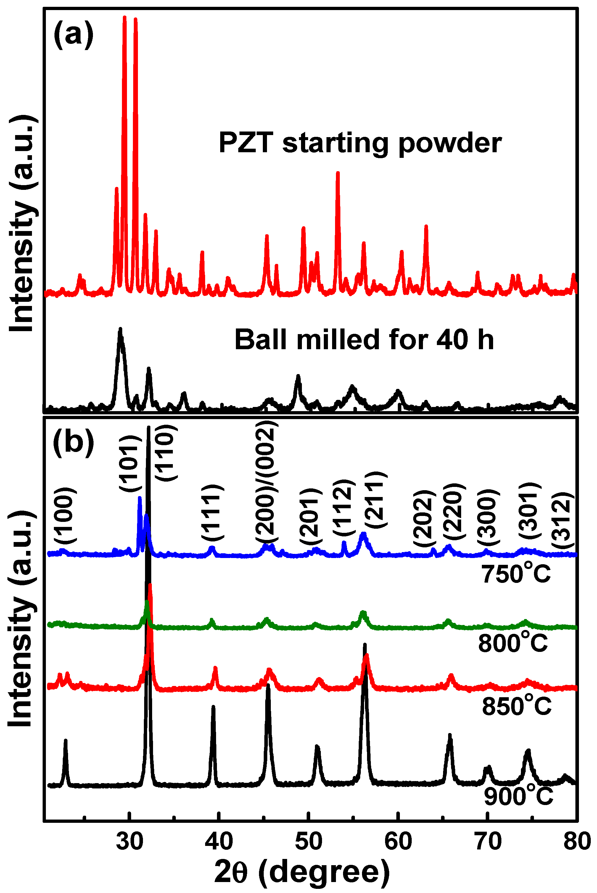
XRD patterns of the PZT starting raw powders—milled for 40 h and followed by SPS sinter at different temperatures—are shown in
Figure 1. PbZr
0.52Ti
0.48O
3 was used as atmospheric powder in the present study.
Figure 1a shows the XRD patterns of all the starting powder peaks for the mixture of PbO, ZrO
2, and TiO
2 commercial powders.
Figure 1a also shows that the perovskite PZT phase was formed from the mixture of raw powders after 40 h of ball milling. Once the powder was ball milled for 40 h, XRD started to show peak broadening, which indicates a reduction in crystallite size. At this point, the majority of sharp peaks of started oxides were reduced. An almost single perovskite PZT phase can be obtained in the sample milled for 40 h. It can also sinter at different temperatures (
Figure 1b). There was no obvious change in the PZT phase with the increasing sintering temperature, but both peak strength and height were increased, and some diffracted peaks were diffused. The strongest peak was at 2θ = 29°—corresponding to the PbO (101) peak—which is a sharp peak before the ball milling treatment. The second-largest broadened peak, at 2θ = 31°, was newly formed and is assigned to the PZT perovskite phase. This observation implies that the conversion from mixed oxides to perovskite PZT phase occurs step by step via the sintering process [
28]. As the sintering temperature increased from 750 to 900 °C, the perovskite peaks height was also increased. The XRD in
Figure 1b shows the (111) pattern as well as (002) and (200) reflections for the tetragonal phase. No peak of other phases except those of the PZT perovskite one was identified in all the XRD patterns, so it is believed that the variation of the Pb content in SPS samples due to sintering can be neglected—thus, the chemical composition of the samples was considered identical. Previous investigations on PbO-based ceramics showed that the Pb content in such materials sintered by SPS at 1000 °C for 3 min was almost the same as that of the sample densified by a conventional sintering [
23]. Since the SPS samples in this study were sintered at a lower temperature than in Reference [
23], any Pb loss during SPS should be within the range of those values. It was suggested that under the condition of vacuum, the lead volatization during the sintering led to a part of the perovskite phase to decompose into the pyrochlore phase [
4,
6,
26].
3.2. SEM Analysis
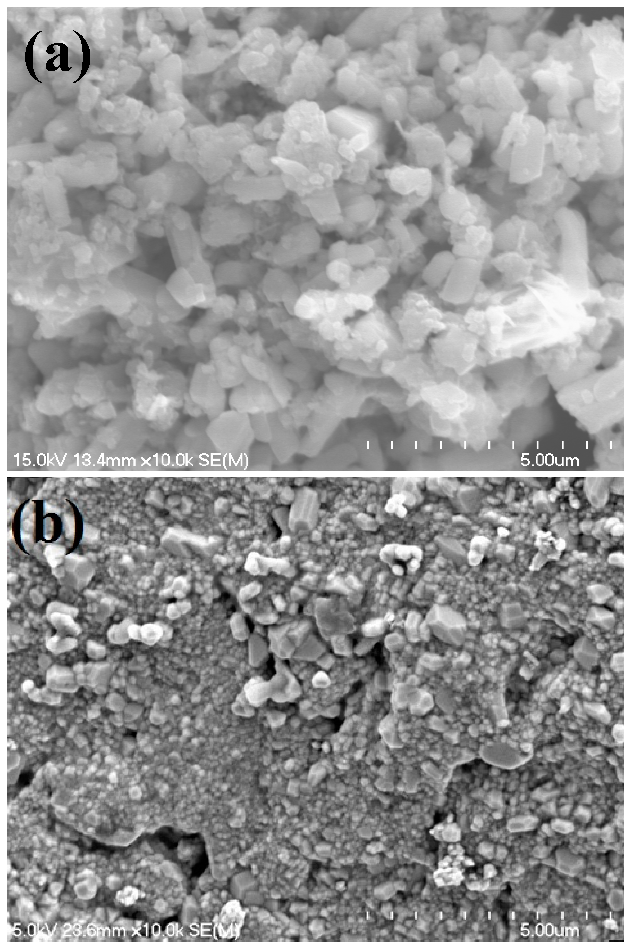
The purpose of ball milling in the present work was to thoroughly mix the starting powders and reduce the particle sizes for subsequent SPS.
Figure 2a shows the scanning electron micrograph of the mixture of PbO, ZrO
2, and TiO
2 powders. After ball milling for 40 h, all the particles were broken into grains and reduced to less than ≈300 nm (
Figure 2b). This reduced small grain enhanced the sinterability of PZT.
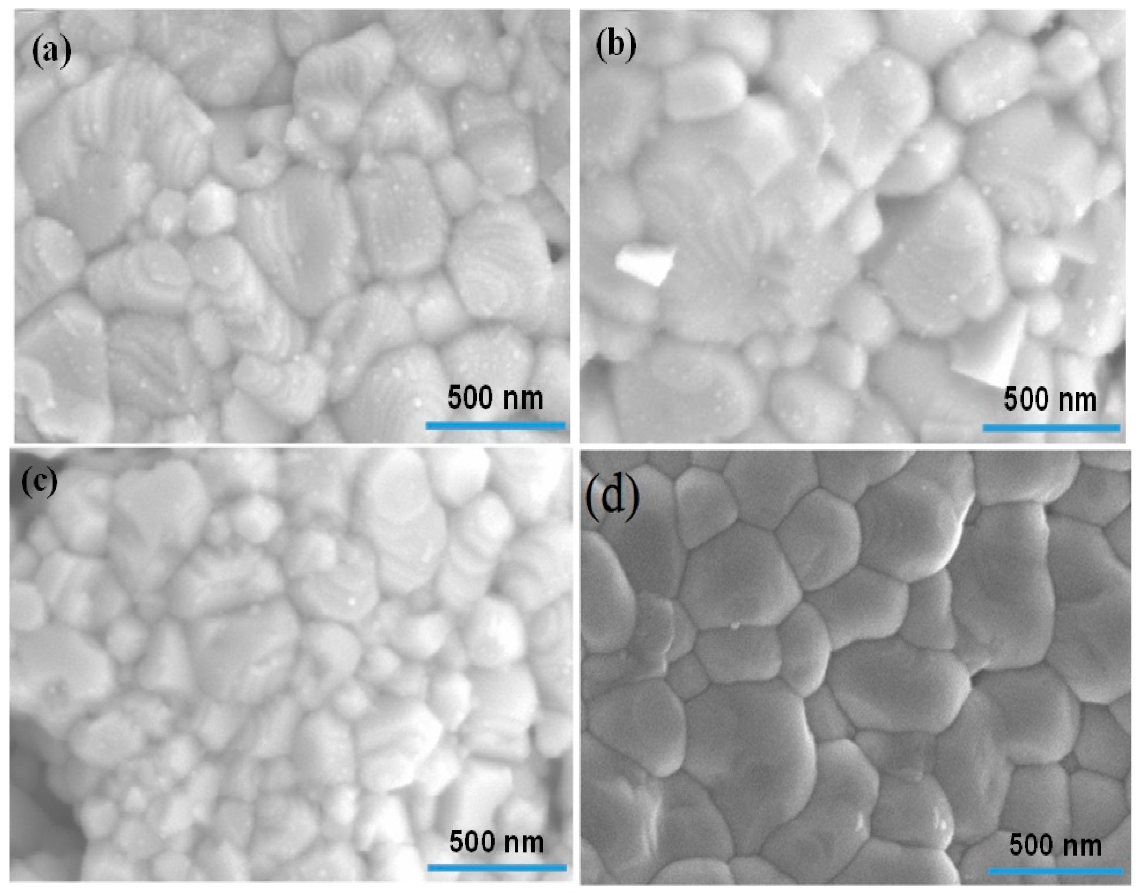
The microstructure of SPS sintered at different temperatures after annealing in the air of the PZT ceramics is shown in
Figure 3a–d. The ceramic microstructure depends on many factors, including technological process, types of fundamental materials, kinetics of phase transitions, sintering time, and grain growth conditions, among others.
The samples show uniform microstructure, and the average grain size increases with increasing sintering temperature, but they are smaller than ≈300 nm. This could be due to lower sintering temperature as well as the shorter soaking time employed in the SPS method. One of the merits of this SPS method is the application of mechanical pressure, which aids in removing pores and enhancing the diffusion. These samples clearly show that some particles are still growing with polygonal shapes, whereas the 900 °C sample show clear and uniform grains in the microstructure, which means these (750 to 850 °C) sintering temperatures are not sufficient.
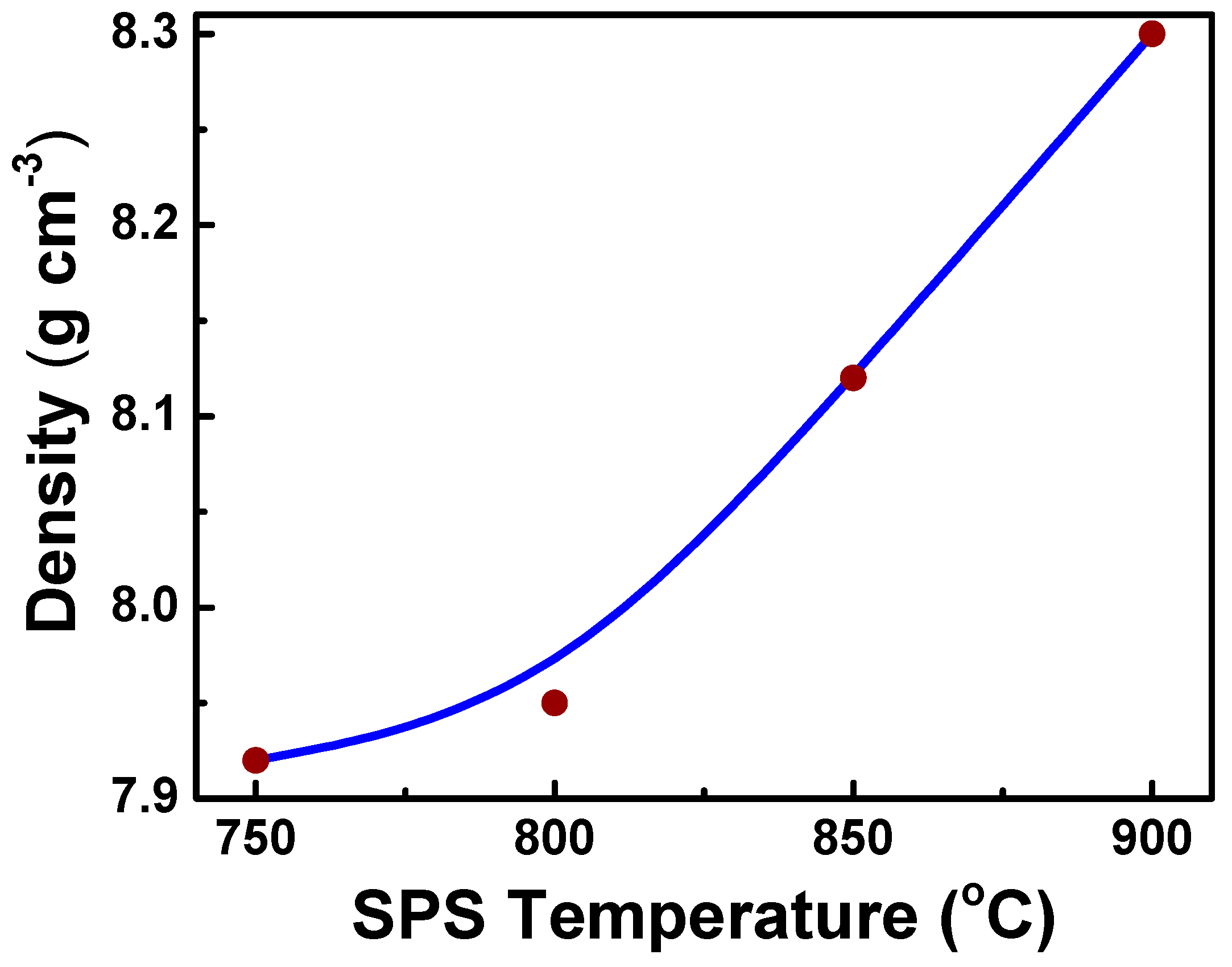
As the sintering temperature increased from 750 to 900 °C, the rate of growing grain percentage was increased and got high dense ceramics with fine grains. Experimental density was measured by the standard water immersion method for the PZT nanoceramics prepared by different SPS sintering temperatures (see
Figure 4). The values of d
exp found that the density increases from 7.92 to 8.30 g cm
−3 as the SPS sintering temperature increases. These values are higher than our previous PZT ceramics sintered by both microwave and conventional sintering process [
1]. Owing to the fact that the 900 °C-SPS-prepared sample had best combination of phase purity, density, and microstructure, it was used to compare with the other SPS samples. The grain size gradually increased when the SPS temperature rose from 750 to 900 °C, which is similar to the grain size in the sample which was sintered normally by Wu et al. [
15]. Compared with other sintering methods, SPS has many advantages, such as the fact that the microscopic electric discharges play a main role in lowering sintering temperature and shortening sintering time.
3.3. Dielectric Measurements
During the present work, SPS sintered samples with better than 99% of the theoretical values were prepared. The sintering parameters were varied in a range as wide as possible in order to obtain different grain sizes. The failure to achieve larger grains was due to the grain-growth inhibition induced by SPS sintering temperatures and short periods.
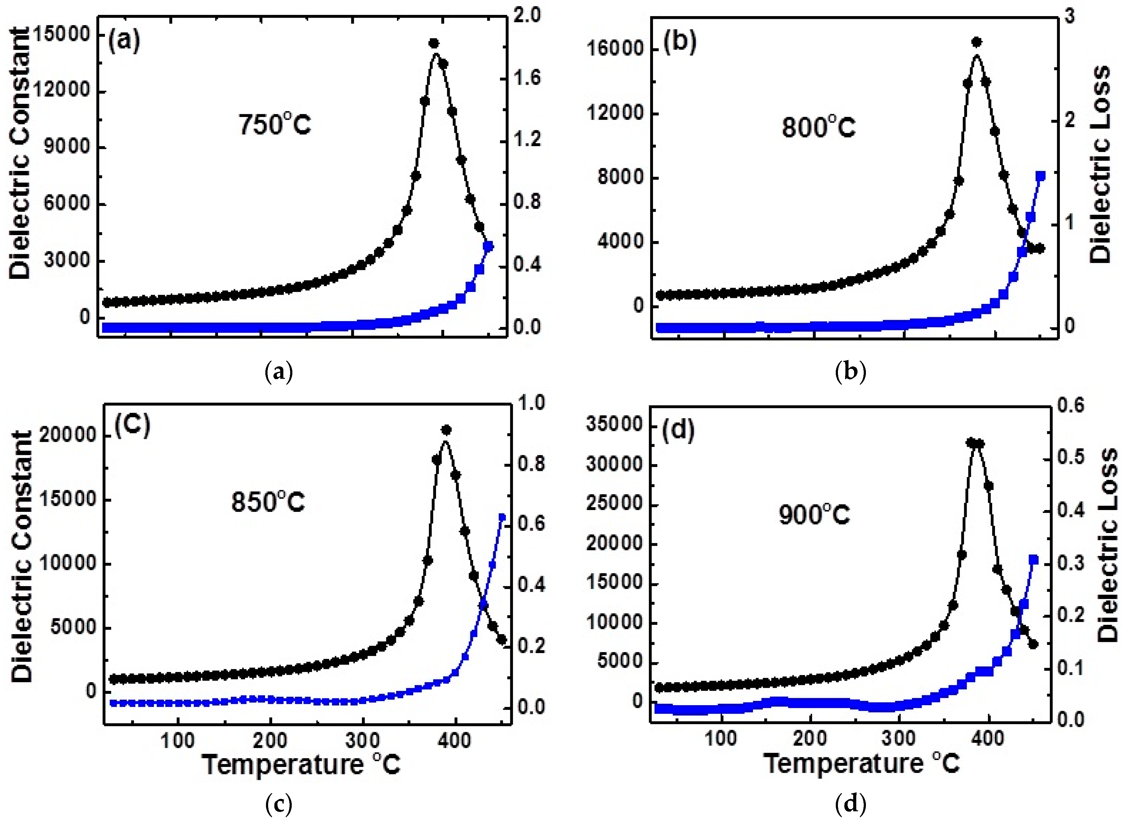
Figure 5 shows the temperature dependence (30 to 450 °C) of the dielectric constant and dielectric loss for the PZT ceramics measured at 100 kHz.
As expected, the dielectric constant shows the maximum at transition temperature and decreases with further increases in temperature. The dielectric anomaly is clearly observable for all the samples, which indicates a ferroelectric behavior. As is well known, the dielectric anomaly can be ascribed to a ferroelectric phase (tetragonal) to paraelectric phase (cubic) transition temperature at
Tc, and it is also apparent that the transition temperature is around 390 °C for all the SPS sintered samples. The room temperature values increased with SPS sintering temperature. The dielectric constant values were 705, 824, 992, and 1863 for 750, 800, 850, and 900 °C samples, respectively. The dielectric constant at
Tc of the PZT samples sintered at 750, 800, 850, and 900 °C was 14,500, 16,500, 20,500, and 33,000, respectively. These values are higher than those reported by Wu et al. on PZT ceramics [
15]. The dielectric constant of the nanocrystalline samples is remarkably less sensitive to temperature in contrast to the coarse ceramics.
As reported previously, the Curie transition temperature of the investigated composition is around 390 °C [
1]—where the permittivity reaches a maximum—accompanied by a minimum of dielectric loss around this temperature. The difference in microstructures, grain size, relative density, and relative porosity of SPS samples should also contribute to the differences in their properties. The influence of grain size on the permittivity of PZT-based ceramics was also previously reported for materials with a grain sizes range. Wu et al. also observed similar behavior in dielectric constants in the same composition with different heat treatment [
15]. The 1100 °C and/or 1 h heat treated SPS prepared PZT ceramic shows the dielectric constant at
Tc is 8000. Chen et al. [
18] investigated a similar sample of SPS followed by high energy ball milling. The maximum dielectric constant at
Tc is about 16,000. Martirena [
29] also discussed about the grain size effect on various ferroelectric materials and suggested that the grain size can affect the ferroelectric properties of ceramics in two ways. One of them is by restricting the motion of domain walls, which are known to contribute to the dielectric constant, piezoelectric, and elastic properties. The second one is by affecting the behavior of each grain taken as a single-crystal single domain. It will be shown that these two factors affects are active at different grain sizes [
30,
31].
SPS is the adapted sintering tool for producing well defined ceramics with small grains in the short sintering time of experiments performed at relatively low temperatures (compared to the conventional sintering process). Takeuchi et al. [
32,
33,
34] obtained sintered pellets with an average grain size of less than 1 μm, exhibiting a room temperature permittivity of 10,000 at 1 kHz. Li et al. [
35] reported the effect of sintering temperature, holding time, heating rate, and synthesis method on grain size and density. Luan et al. [
36] completed the study by HRTEM observations showing 180° ferroelectric domains and some twins in some ferroelectric materials. The large values of dielectric constants in PZT-based materials are due to unusual increases in wall mobility due to the Pb vacancies, which release some interdomain stresses between 90° walls [
31]. Domain wall displacement causes the dielectric loss and dielectric constant in the ceramics and thin films, particularly near the phase transition temperatures [
37]. The grain size, crystallographic orientation, crystal structure, electric field, preparation conditions, and processing parameters also affect the domain wall displacement in the thin films and ceramics.
3.4. Ferroelectric (P-E Loop) Properties
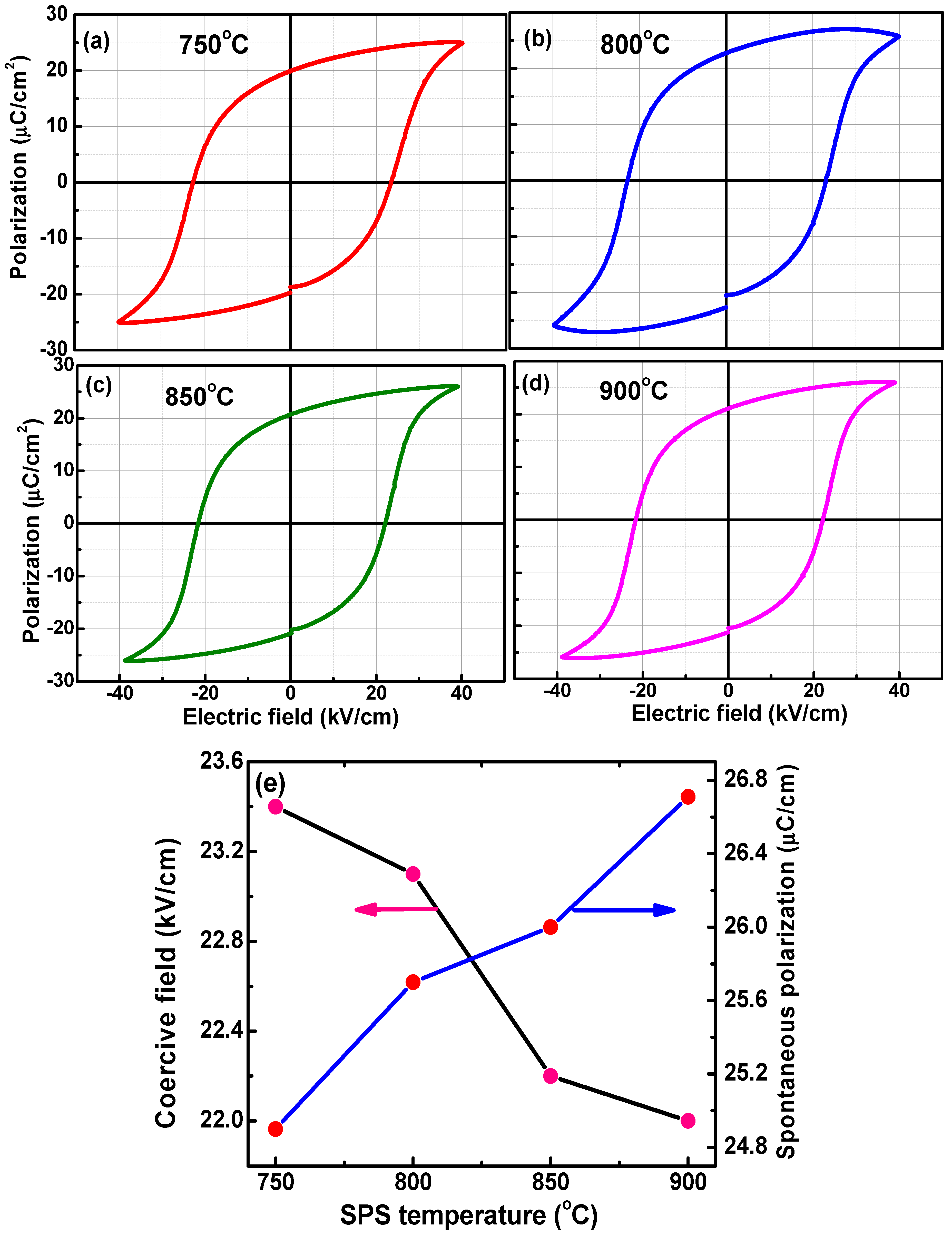
The comparison of the room temperature polarization vs. electric field hysteresis loops of the ceramics sintered at different temperatures is depicted in
Figure 6. All the samples showed well-saturated typical ferroelectric hysteresis loops, and the values of remnant polarization (
Pr), coercive filed (
Ec), and saturations polarization (
Ps) were higher than our previous microwave sintered PZT [
1].
Ec and
Pr were taken from the positive intercept of the ferroelectric hysteresis loops at zero polarization. As the grain size decreased, the saturation polarization decreased and the coercive filed increases (see
Figure 6e), which implies that the SPS samples were becoming more easily polarized under the applied electric field [
37]. Another phenomenon is that the samples sintered at 750 and 800 °C, the positive coercive field, positive remnant polarization, and their negative counterparts are asymmetric about the original point. According to Li et al. [
38], the uneven pinning of the domains in these samples contributes strongly to the asymmetric shape of the PE loops. Because the domain walls in ferroelectrics are relatively thin, they can be pinned by point defects or charged species such as electrodes, which may diffuse into charged domain walls. Other pinning effects are associated with the fields created inside the grains by electric fields and/or elastic dipole defects [
39,
40].
3.5. Piezoelectric (d33) Properties
The sintered ceramic samples were placed in a poling instrument and polarized at high field in silicone oil, which kept the temperature constant (180 °C for 1 h). The ratio of voltage elevation was about 1 kVs
−1. After poling the applied voltage was lowered to zero, keeping the temperature high. The charge was freed by short circuiting both electrodes after cooling.
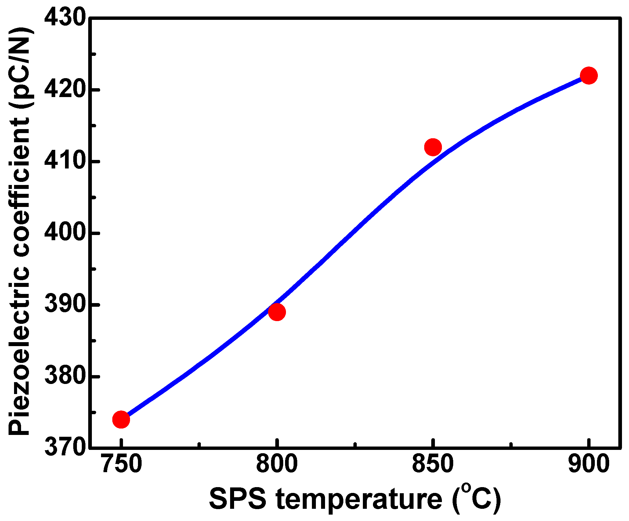
Figure 7 shows the variation of the piezoelectric constant
d33 for the PZT ceramics sintered at different SPS temperatures. It is well known that all the PZT ceramics show higher piezoelectric constant values in comparison to literature. In general, the piezoelectric properties at room temperature increase with increasing grain size.
The piezoelectric constant increased almost linearly from 374 pC/N for the 750 °C sintering to 422 pC/N for 900 °C sintered sample. The piezoelectric constants of the ceramics usually determined by the grain size, crystal structure and density. A study by Shao et al. [
41] indicated that for the conventional sintered BaTiO
3 ceramics with larger grain size, the piezoelectric constant decreases from 419 to 185 pC/N when the average grain size increases from 7 to 19 μm. By the model proposed by Okazaki and Nagata [
40], as the grain size increases, the grain boundary phases—which are directly related to the volume of the space-charge regions—get smaller and finally result in improving the piezoelectric properties for eliminating the clamping effect on the motion of domain walls. It can be concluded that the internal bias field effect became more dominant than that of the grain size effect, which deteriorated the piezoelectric properties for the ceramics sintered between 750 and 900 °C.
4. Summary
PZT nanocrystalline ceramics with various grain sizes were prepared by high energy ball milling followed by spark plasma sintering temperature techniques. The SPS sintering temperature varied from 750 to 900 °C for 5 min. The experimental density was measured by standard water immersion Archimedes’ method for the PZT nanoceramics prepared by different SPS sintering temperatures. Experimental density values of dexp found that the density increases from 7.92 to 8.3 g cm−3 as the SPS sintering temperature increases. These values are higher than our previous PZT ceramics sintered in both microwave and conventional process. X-ray diffraction analysis showed single phase with tetragonal perovskite structure, but there is almost no influence of the impurities in the present research study. As the SPS temperature increased, the dielectric constant and ferroelectric properties increased and influenced the domain wall contribution to the grain size effects observed. The room temperature dielectric constant values increased with SPS sintering temperature. The dielectric constant was 705, 824, 992, and 1863 for 750, 800, 850 and 900 °C samples, respectively. The dielectric constant at Tc of the PZT samples sintered at 750, 800, 850, and 900 °C was 14,500, 16,500, 20,500, and 33,000, respectively. The values of remnant polarization (Pr), coercive filed (Ec), and saturations polarization (Ps) were higher than our previous microwave sintered PZT. The values of the polarization and the coercive field of the sintered samples were found to be increasing and decreasing, with an increase of SPS temperature from 750 to 900 °C. The piezoelectric constant increased almost linearly from 374 pC/N for the 750 °C sintered sample to 422 pC/N for the 900 °C sintered sample. The advanced sintering technique involving the internal bias field effect and the grain size effect affected the dielectric, piezoelectric, and ferroelectric properties of nano PbZr0.52Ti0.48O3 ceramics.


