1. Introduction
As integrating smaller-sized high performance electronic devices has become a key point over the past few decades, innovative transistor designs have emerged. Chip-to-wafer density has to remain high to be competitive, so size reduction is still a burning issue, and non-planar devices are part of these brand new products. As a consequence, multi-gate field-effect transistors (FET) have been developed. In such a new gate architecture, silicon nanowires (SiNWs) FETs seem to be one of the most attractive choices. They enable avoiding problems due to the short channel effect, such as threshold voltage or drain-induced barrier lowering. More precisely, surrounding-gate transistors where the gate encircles the nanowire channel allow a better electrostatic gate control. SiNW transistors of diameters even down to 3 nm have already been prepared, during these years, by various experimental groups [
1,
2]. Silicon nanowires are quasi-one-dimensional structures in which the electrons are spatially confined in two directions, and they are free to move along the axis of the wire. The nonequilibrium Green’s function (NEGF) formalism is a more advanced transport model for the simulation of SiNW, as it takes into account the wave nature of electrons. The NEGF formalism necessitates rather intensive computational efforts, since it requires detailed information on the propagation of the electron wave packet injected in the device, and microscopic scattering mechanisms other than electron-phonon interactions are difficult to incorporate because the corresponding self-energy terms are usually nonlocal functions of the spatial coordinates.
However, the main quantum transport phenomena in SiNW at room temperature, the source-to-drain tunneling and the conductance fluctuation induced by the quantum interference become significant only when the channel lengths of the SiNW are smaller than 10 nm [
3]. Therefore, for longer channels, semiclassical formulations based on the 1D multi-sub-band Boltzmann transport equation (MBTE) can give reliable terminal characteristics when it is solved self-consistently with the 3D Poisson and 2D Schrödinger equations in order to get the self-consistent potential, sub-band energies and wavefunctions. In the literature, the numerical solution of the MBTE has been obtained using Monte Carlo simulations [
4,
5,
6,
7,
8] or deterministic solvers [
6,
9] at the expense of large computational effort and statistical noise [
10,
11,
12].
Another alternative is to obtain from the MBTE hydrodynamic models that are a good engineering-oriented approach. This can be achieved by taking the moments of the MBTE and by closing the obtained hierarchy of balance equations, as well as modeling the production terms (i.e., the moments on the collisional operator). The closure problem can be tackled by means of the maximum entropy principle (MEP) of extended thermodynamics [
13,
14,
15], in which the distribution function used to calculate the higher-order moments and the production terms is assumed to be that which maximizes the entropy under the constraints of the given set of moments. We want to underline that the distribution function obtained with the MEP is an approximation of the real one, but from the other side, this distribution is useful to determine analytically without any fitting procedure the higher-order moments and the production terms. In this way, a hydrodynamic model has been obtained with a simplified band structure [
16,
17,
18,
19].
The goal of this paper is to set up a consistent hydrodynamic model compatible with the real band structure dictated by atomistic simulation models. The plan of the paper is the following: in
Section 2, the electronic band structure is introduced; in
Section 3, the quantum confinement is discussed, and the main scattering mechanisms are treated in
Section 4; in
Section 5, we introduce the kinetic and hydrodynamic models; in
Section 6 closure relations are obtained using the MEP; finally, in
Section 7, the low-field mobility for a gate-all-around SiNW transistor has been evaluated, and conclusions are drawn in
Section 8.
2. Electronic Band Structure
In bulk silicon (Si), the lowest conduction band is formed by six equivalent valleys near the
X-point of the Brillouin zone. In this case, we have an indirect band-gap of 1.143 eV at ± 0.85
in the Δ direction with
0.19,
0.98 (units electron mass) and lattice parameter
= 5.43 Å [
20]. In SiNW, the band structure is altered with respect to the bulk case depending on the cross-section wire dimension, the atomic configuration and the crystal orientation. The atomistic modeling is able to capture the nanowire band structure, including information about band coupling and mass variations as functions of quantization [
3,
21,
22,
23,
24]. Atomistic simulations are more appropriate for nanowires of a few nanometer cross-sectional sides, due to the high variability of the involved parameters. However, for SiNW with cross-sections greater than 3 nm, atomistic simulations using the tight-binding (TB) approach show that the band structure is more stable [
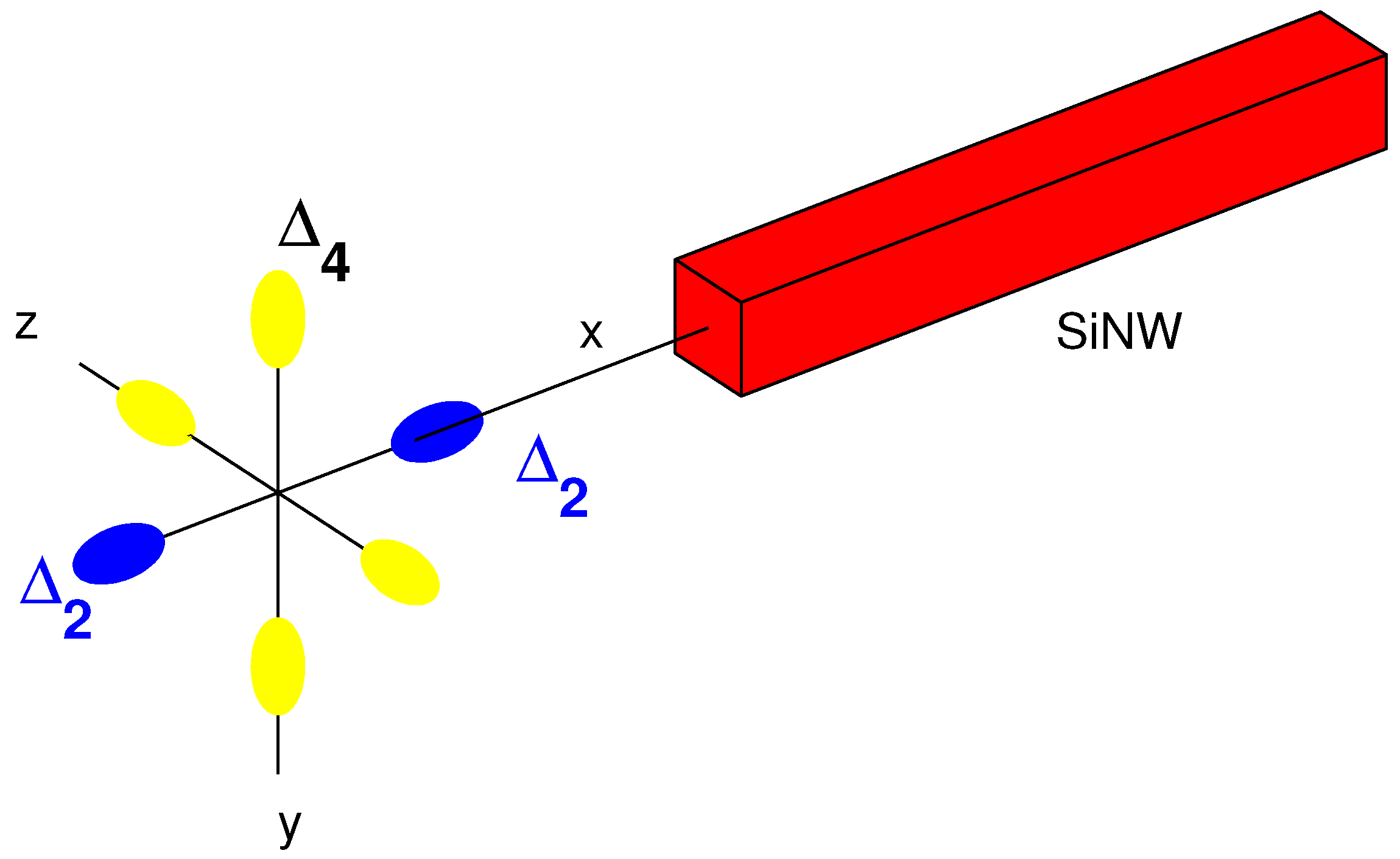
21]. For a rectangular SiNW with longitudinal direction along the
crystal orientation, confined in the plane
, the 1D Brillouin zone is 1/2 as long as the length of the bulk Si Brillouin zone along the Δ line (i.e.,
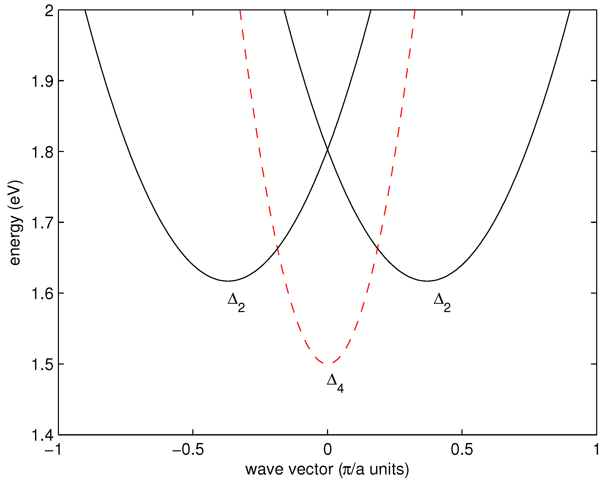
). The six equivalent Δ conduction valleys of the bulk Si are split into two groups because of the quantum confinement (see
Figure 1). The sub-bands related to the four unprimed valleys
(
and
orthogonal to the wire axis) are projected into a unique valley in the Γ point of the one-dimensional Brillouin zone. Therefore, a SiNW is a direct band-gap semiconductor. The sub-bands related to the primed valleys
(
along the wire axis) are found at higher energies and exhibit a minimum, located at
(see
Figure 2), and the energy gap between the
and
bottom valley is 117 meV. From the energy dispersion relation
obtained from the TB, one can evaluate the effective mass
in the parabolic spherical band approximation, i.e.,
obtaining
0.94,
0.27. Non-parabolic correction to Equation (1) can be introduced [
3,
25,
26], but the fitting parameter depend heavily on the particular atomic configuration.
3. Quantum Confinement
In an ideal quantum wire, the system is assumed sufficiently long along the axis of the wire that translational invariance holds. For a quantum wire with linear expansion in the
x-direction and confined in the plane
y-
z, the normed wave function
can be written in the form:
where
is the valley index (one
valley and two
valleys),
the sub-band index,
is the wave function of the
l-th sub-band and
-th valley and the term
describes an independent plane wave in the
x-direction confined to the normalization length,
, with wave number
. Let us consider a set of conduction electrons moving in the wire. Any one electron will react to the confining potential
and to the presence of all other free electrons in the system. The simplest approximation that takes into account the presence of many electrons, called Hartree approximation, is to assume that the electrons as whole produce an average electrostatic potential
, and that a given electron feels the resulting total potential energy
, i.e.,
where
e is the absolute value of the electric charge. The spatial confinement in the
plane is governed by the Schrödinger–Poisson system (SP):
Equation (4a) is the Schrödinger equation in the effective mass approximation (EMA), which has been proved adequate down to the 3-nm wire width [
27]. Equation (4c) is the Poisson equation, where
is the absolute dielectric constant (8.854 × 10
C/(V·m));
is the relative dielectric constant (11.7 for Si, 3.9 for
; and
are the assigned doping profiles (due to donors and acceptors). The electron density
is given by Equation (4d), where
is the linear density in the
-valley and
l-sub-band, which must be evaluated by the transport model (hydrodynamic/kinetic) in the free movement direction. In the following, we shall assume that the cross-section Ω of the wire is surrounded by an oxide, which gives rise to a deep potential barrier,
where 3.1 is the height of the energy barrier at the Si-
interface.
The SP system forms a coupled nonlinear Partial Differential Equations, which it is usually solved by an iteration between Poisson and Schrödinger equations. Since a simple iteration by itself does not converge, it is necessary to introduce an adaptive iteration scheme [
28]. The solution gives the electrostatic potential
, as well as the eigenvalues (or sub-band energies)
and the eigenvectors (or electron envelope wavefunctions)
as a function of the unconfined
x direction.
Finally, the total electron energy in the
-valley and
l-sub-band is:
where
is the bottom of the conduction band and
α is the non-parabolicity factor (zero in the parabolic case).
4. Carrier Scattering
Essential for the description of any particle transport with a semiclassical approach is the definition of the transition rate w(
k, k’), which represents the probability that an electron with wave number vector
, due to a scattering, passes into a state with wave number vector
in the unit time. In the SiNW case:
representing the probability per unit time that the state
becomes the state
:
The transitions rate fulfill Fermi’s golden rule, i.e.,
where
is the perturbation potential,
is the total energy (6a) and it includes thus the possibility of inter-sub-band scattering processes. The term
enables that a particle of wave vector
is involved in the scattering process (the plus stands for absorption and the minus for emission).
4.1. Electron-Phonon Scattering
The perturbation potential
is caused by a deformation potential and writes [
29]:
where
is the mass density,
the crystal volume,
is the phonon distribution function involved in the scattering,
the phonon energy obtained from the phonon dispersion relation for Si (bulk in our case) and:
The scattering mechanism can drive one electron in the same valley (intra-valley) or in a different valley (inter-valley). In bulk silicon, the intra-valley scattering involves only acoustic phonons (two types, LA and TA), and they are evaluated using the first order approximation (with the Debye approximation
[
20]). The inter-valley scattering is due to six types of phonons: three of the g-type, when electrons scatter between valleys on the same axis, or of the f-type, when the scattering occurs between valleys on perpendicular axes, and they are evaluated in the zero order approximation (using the Einstein approximation with
constant).
For SiNW, we shall consider bulk phonons and follow the bulk Si scattering selection rules. According to bulk Si scattering selection rules, the elastic processes (due to elastic phonons, surface roughness scattering, impurity scattering) are only intra-valley, whereas the inelastic ones (due to inelastic phonons) are only inter-valley [
24].
Since in SiNW, the six conduction valleys reduce to a three-valley model, the valley index
assumes the value
(for the unprimed valleys) and
(for the two primed valleys). However, the two valleys
are symmetric with the same mass (see
Figure 2), and then, they can be considered equivalent. Hence, in the following, we shall deal with a two-valley model, the valley
and the valley
. This equivalence in the valleys introduces the following scattering rules
The intra-valley elastic scattering rate (acoustic in the equipartioned case) is given by [
30]:
For inter-valley scattering, supposing the phonons to be in thermal equilibrium, one obtains:
where
is the bottom of the energy valley,
is the the number of possible final equivalent valleys for the type of inter-valley scattering under consideration,
is the Bose–Einstein distribution, i.e.,
where
is the lattice temperature, and
is the form factor:
For intra-valley inelastic scattering, Equation (13) is still valid supposing to have
, i.e.,
All parameters are listed in
Table 1.
4.2. Scattering with Impurities
This process is dominant at low temperatures. For an impurity located in the position
, with charge
, in the unscreened case, we have:
Then, one obtains [
30]:
where
, and
is the modified Bessel function.
Since this process is elastic and intra-valley, from Equation (8) for the i-th impurity, we obtain:
where:
For the sake of simplicity, we shall assume that the impurities are distributed uniformly along the wire, i.e., they are located in
, and in the parabolic band approximation, we get:
where
is the impurities number per unit length and
the Heaviside function.
4.3. Surface Roughness Scattering
Surface roughness scattering (SRS) in silicon nanowires is the key scattering mechanism, as it yields a very strong dependence of the low-field electron mobility on the silicon body diameter, as well as on the effective field.
In the case of perfectly smooth Si-
interface, the electron wavefunctions and energy level of each sub-band are obtained by solving the Equation (4a) in each
x-cross section, with:
where
U is the confining potential,
the effective potential composed by
the electrostatic potential energy (satisfying the Poisson equation),
the image potential due to the mismatch of the dielectric constants between Si and
and
the exchange-correlation energy due to the electron-electron interaction. However, practically, one must take into account the roughness surface.
Let us consider the wire interface along the x-z plane (whose normal is the y-direction). Then, is a random function, which describes the deviation of the actual interface from the ideal flat interface. This fluctuation modifies directly the barrier potential U, and it induces a change in the other potentials. Therefore, the sub-band wave functions and energy bands depend explicitly on x.
For the 1D confinement (e.g., the quantum well), the first order complete theory can be found in [
31]. In the case of infinite confining potential, the main results is (see Figure 4 in [
31]) that for silicon thickness greater than 8 nm, the SRS mobility converges to the SRS bulk mobility, and moreover, the contribution of
can be neglected. Following [
4,
30], we shall consider a simpler SRS model, where:
are neglected (which of course is true for silicon thickness greater than 8 nm);
SRS accounts for deformations only for the potential (not the wave functions);
fluctuation depends only on x, i.e., ;
the perturbation in the potential is only in the y-variable, i.e., .
If we expand the potential in the
y variable (with
constants), up to the first order in
, we get:
Then, finally, the SRS matrix element is:
The SRS is an intra-valley scattering mechanism, and it depends on the electric field normal to the surface. Since the cross-section of our wire is a rectangle, we have two contributions, one along the
y-direction and the other along the
z-direction. Hence,
Assuming exponentially correlated surface roughness, in the parabolic band approximation, one obtains [
4]:
where
and
are the rms (root mean square) height and the correlation length of the fluctuations at the Si-
interface, respectively (see
Table 1),
and
are given by Equation (27).
The contribution for is similar to Equation (27), supposing to change .
5. Kinetic and Hydrodynamic Model
In low-dimensional systems, we consider the lattice with perfectly smooth boundaries, free of impurities or other random inhomogeneities. In such an ideal system the energy levels due to disorder are small, so that crystal momentum conservation is approximately preserved. In this framework, we can then construct a kinetic equation in which the distribution function evolves in time under the streaming motion of external forces and spatial gradient, and the randomizing influence of nearly point-like (in space-time) scattering events. For devices with a characteristic length of a few tens of nanometers, the transport of electrons along the axis of the wire can be considered semiclassical within a good approximation; otherwise, a quantum-kinetic approach must be used [
32]. The distribution function for the electrons in a quantum wire, with linear expansion in
x-direction, depends on the
x-direction in real space, the wave vector in
x-direction
and the time
t, i.e.,
for the valley
and sub-band
l. The MBTE reads [
30]:
where
ℏ is the Planck constant divided by
,
the electron group velocity and
the effective field:
The RHS of Equation (29) is the collisional operator, which is split into two terms modeling respectively intra-valley (with
) and inter-valley transitions (with
). In the low density approximation (not degenerate case), the collisional term for the
η-th scattering rate writes:
where
for the acoustic, SR and inelastic (intra-valley) scattering,
for the inter-valley scattering. Starting from the kinetic Equation (29), one can obtain balance equations for macroscopic quantities associated to the flow. By multiplying (29) by a weight function
and integrating over
, one finds:
where:
are the moments relative to the weight functions
. By integrating by parts and supposing that
f tends to zero sufficiently fast as
, we obtain:
We have chosen a four-moments model with:
and one obtains from Equation (34) the following balance equations in the unknown (
):
where:
The production terms for the velocity, energy and energy-flux
,
,
are obtained from
by multiplying the integrand function for
, respectively. From the above definitions, we can introduce the following average quantities:
6. Maximum Entropy Principle and Closure Relations
Since the number of unknowns exceeds the number of equations and the production terms are unknown, closure relations must be introduced. The MEP gives a systematic way for obtaining constitutive relations on the basis of information theory [
13,
14,
15]. Such an approach has been used in the simulation of 2D nanoscale structures [
33,
34] and for simulating the 3D electron transport in sub-micrometric devices, in the case in which the lattice is considered as a thermal bath with constant temperature [
35,
36,
37,
38] or when the phonons are off-equilibrium [
39,
40,
41,
42,
43,
44,
45]. We shall assume that the electron gas is sufficiently dilute, then the entropy density can be taken as the classical limit of the expression arising in the Fermi statistics, i.e.,
According to the MEP, if a given number of moments
is known, the distribution functions
, which can be used to evaluate the unknown moments, correspond to the extremum of the total entropy density under the constraint that they yield the known moments, i.e.,
If we introduce a set of Lagrange multipliers
, the problem to maximize
under the constraints (44) is equivalent to maximizing:
So doing, we shall obtain the following distribution function:
By inserting the previous Equations in (44), we obtain:
which defines implicitly the Lagrange multipliers. In order to invert the above relations, we shall perform an expansion around the thermal equilibrium. In fact, at equilibrium,
must reduce to the Maxwellian. This means:
Then, we consider the vanishing Lagrange multipliers of higher order with respect to equilibrium, by introducing the smallness parameter
τ:
The inversion problem has been tackled in [
16] obtaining, up to the first order in
τ (for simplicity, we shall omit the indexes
):
The Lagrange multipliers are determined by imposing the constraint (4a):
whereas the higher order flux is:
In order to close the system, we need functional relations for the production terms, which can be evaluated by using the MEP distribution Function (49).
6.1. Closure for the Electron Number Production
6.1.1. Evaluation of
This is an intra-valley inelastic scattering mechanism, where the scattering rate is given by Equation (17). After long calculations, one obtains:
6.1.2. Evaluation of
This is an intra-valley elastic scattering mechanism, where the scattering rate is given by Equation (12). We obtain:
where:
and:
6.1.3. Evaluation of
This is an intra-valley elastic scattering mechanism, where the scattering rate is given by: Equation (27). We get:
where:
6.1.4. Evaluation of
This is an intra-valley scattering, where the scattering mechanism is given by Equation (22). We get:
where:
6.1.5. Evaluation of
This is an inter-valley inelastic scattering mechanism, where the scattering rate is given by Equation (13). The result is similar to Equation (58) (obtained for an intra-valley, inelastic scattering) with
, but supposing to change Equation (61) into:
where
is given in Equation (14). Then, we obtain:
6.2. Closure for the Production of Electron Energy
We observe that, with respect to Equations (54)–(57), there is an extra , and by multiplying all of the previous integrals by , similar results hold.
6.3. Closure for the Production of Electron Crystal Momentum
6.3.1. Evaluation of
For this production term, the scattering rate is given by Equation (17). We get:
where:
6.3.2. Evaluation of
This is an intra-valley inelastic scattering rate, where the scattering rate is given by Equation (12). We get:
where:
6.3.3. Evaluation of
This is an intra-valley elastic scattering mechanism, and from Equation (27), we get:
where:
6.3.4. Evaluation of
This is an intra-valley scattering, and from Equation (22), we get:
where:
6.3.5. Evaluation of
This term is similar to Equation (96) (obtained for an intra-valley inelastic scattering), but with
and supposing to change Equation (61) into:
where
is given in Equation (14), we obtain:
where:
6.4. Closure for the Production of Electron Energy-Flux
We observe that, with respect to Equations (92)–(95), there is an extra , and by multiplying all of the previous integrals by , similar results hold.
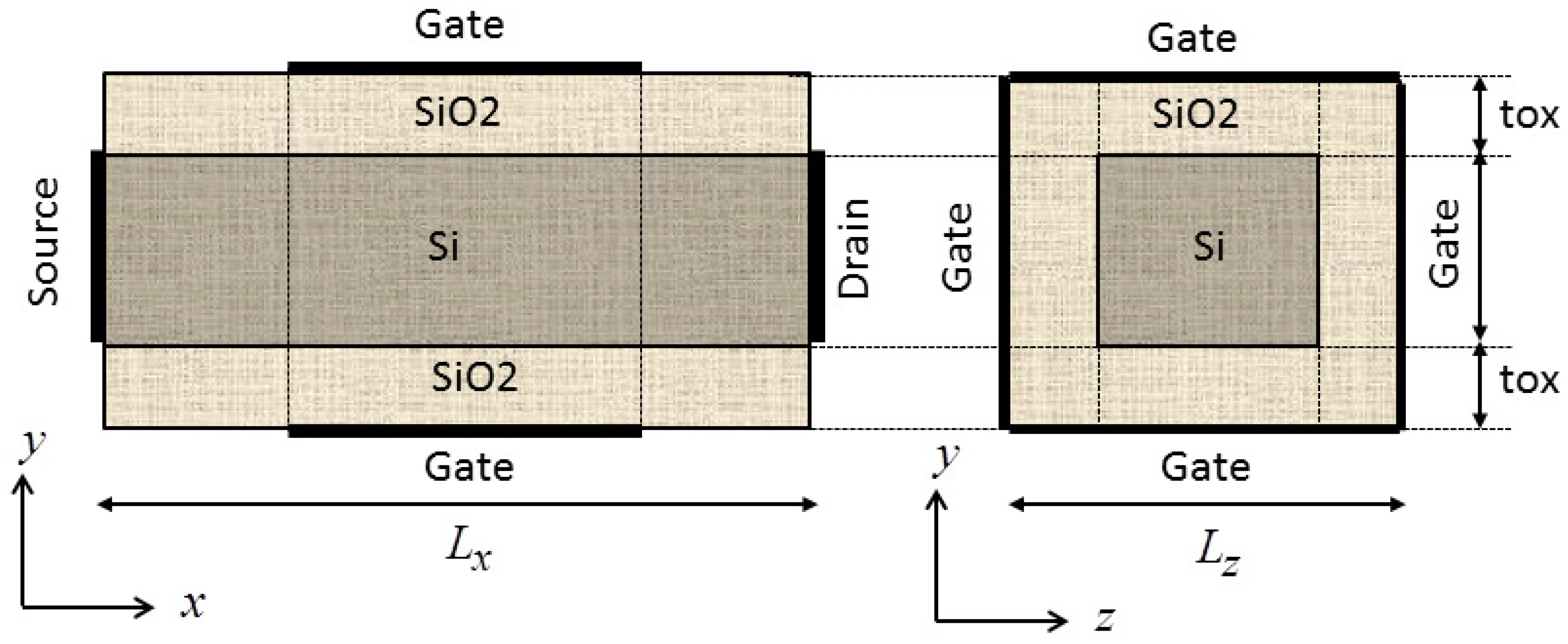
7. Case of Study
As a case of study, we introduce the so-called gate-all-around (GAA) SiNW transistor. This is a silicon nanowire with an added gate wrapped around it, in such a way that we have a three contact device with source, drain and gate (see
Figure 3). Such devices have been designed during these years in order to maintain a good electrostatic control in the channel [
1,
2]. The gate electrode is assumed to be metallic, so that there is no potential drop inside the gate, and depletion effects are not considered. In the following, we shall consider a very simple SiNW transistor having the channel homogeneously doped to
3 ×
and very long (
120 nm) with respect to the transversal dimensions (
nm), where the oxide thickness (
) is tox = 1 nm. In such a case, the moment system reduces to a set of ordinary differential equations with the time as the only independent variable to be coupled to the SP system Equation (4).
First of all, let us consider the thermal equilibrium regime where no voltage is applied to the contacts, i.e.,
and no current flows. Hence, the electron distribution function is the Maxwellian:
where
ν is the Fermi level,
the valley energy minimum,
T the electron temperature, which we shall assume to be the same in each sub-band and equal to the lattice temperature. The condition of zero net current requires that the Fermi level must be constant throughout the sample, and it can be determined by imposing that the total electron number equals the total donor number in the wire. Then, the linear electron density at equilibrium writes:
where the sub-band energies
are obtained by solving the SP system Equation (4) using Equation (139) with
= 0.
Now, we consider the quasi-equilibrium regime, where a very small axial electric field frozen along the channel (1000 V/cm) is applied, and we turn on the gate. The system is still in local thermal equilibrium, the distribution function is the Maxwellian, but some charge flows in the wire. The linear density writes:
where the only difference between Equations (139) and (140) is in the energy sub-bands
, which now are obtained solving the SP system Equation (4) with
V,
V,
V. Once the solution has been obtained, the energies
and wave functions
for each sub-band are fixed and exported into the hydrodynamic model. Moreover, the obtained linear density
is used as the initial condition for this model. The other initial conditions for the balance Equations (35)–(38) are:
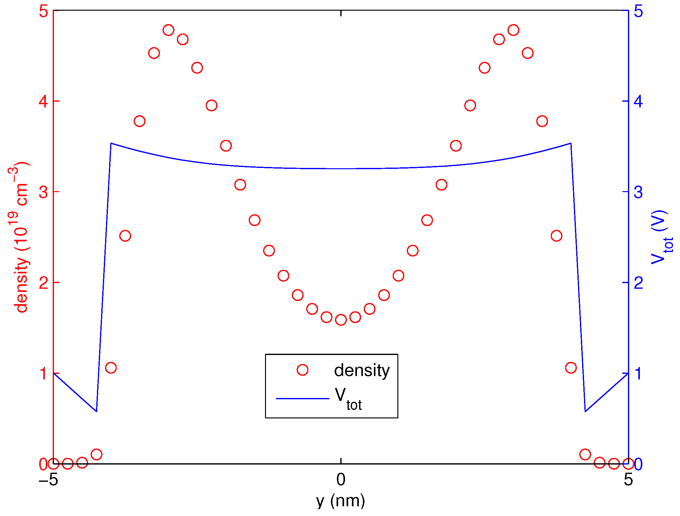
Figure 4 shows the distribution of charge density (4d) and the total potential (3) along the cross-section at
48 nm and
nm. A surface inversion layer is formed, similar to a usual MOSFET channel with the electron density peak 1 nm from the oxide interface. The band-bending at the interface forms the quantum well for the electrons.
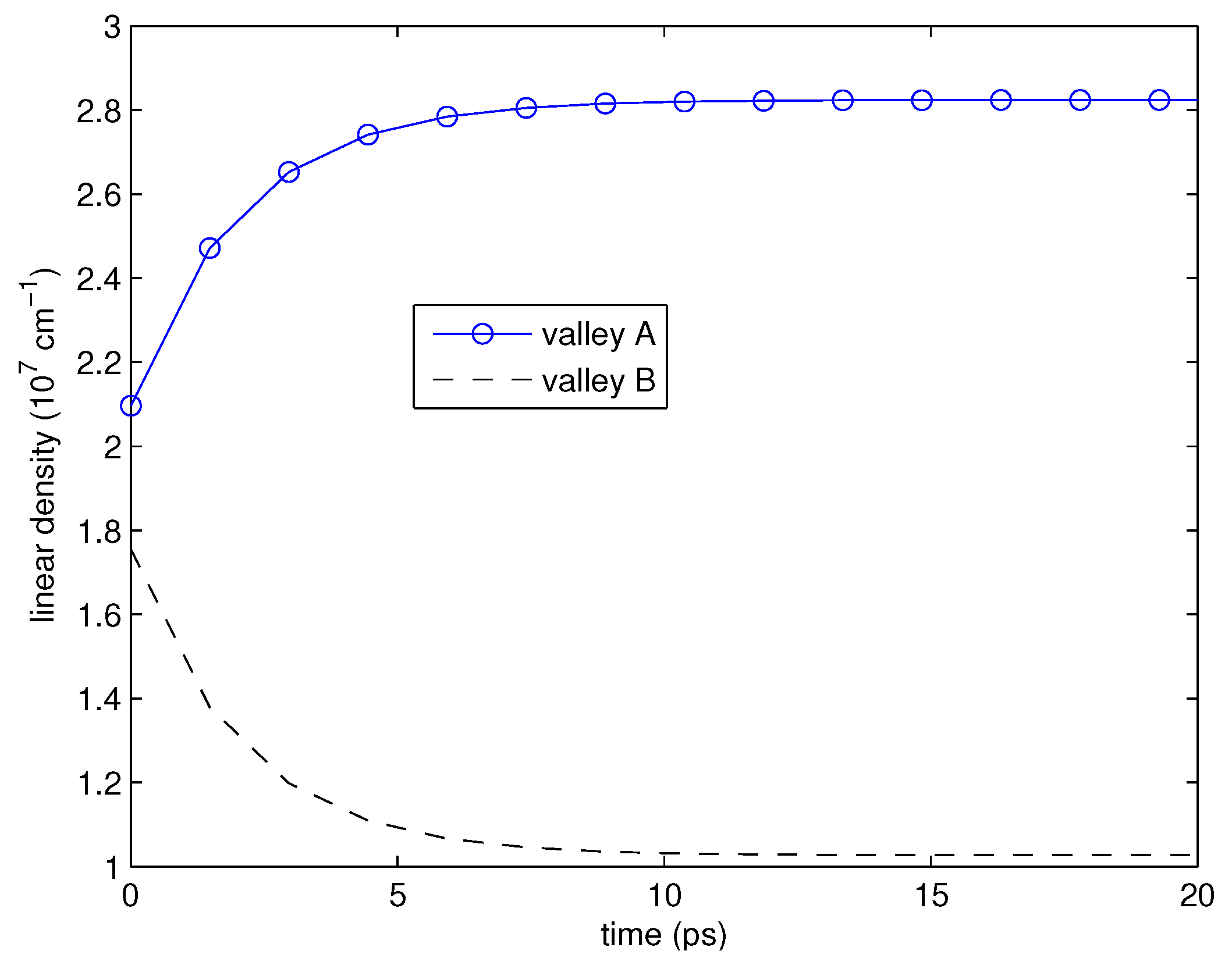
In
Figure 5, the total linear density for the
A and
B valleys (i.e.,
) versus the simulation time is plotted. One can note a depletion of the higher
B valley. In fact, the electrons change valley according to the inter-valley scattering mechanism given by Equation (13). The scattering from
A to
B happens if the electron energy is greater than a certain threshold (related to the energy gap between the two valleys, (i.e., 117 meV), whereas the converse is more probable. If we apply a small electric field (1000 V/cm) in the wire, the electrons, at the beginning of the simulation, cannot gain enough energy to jump from
A to
B, whereas it is more probable that the opposite will happen. As the simulation time increases, the electrons in
A gain enough energy (i.e., they have a slightly increase of the mean energy) to activate the jump from
A to
B, and in the stationary regime, an equilibrium state is reached.
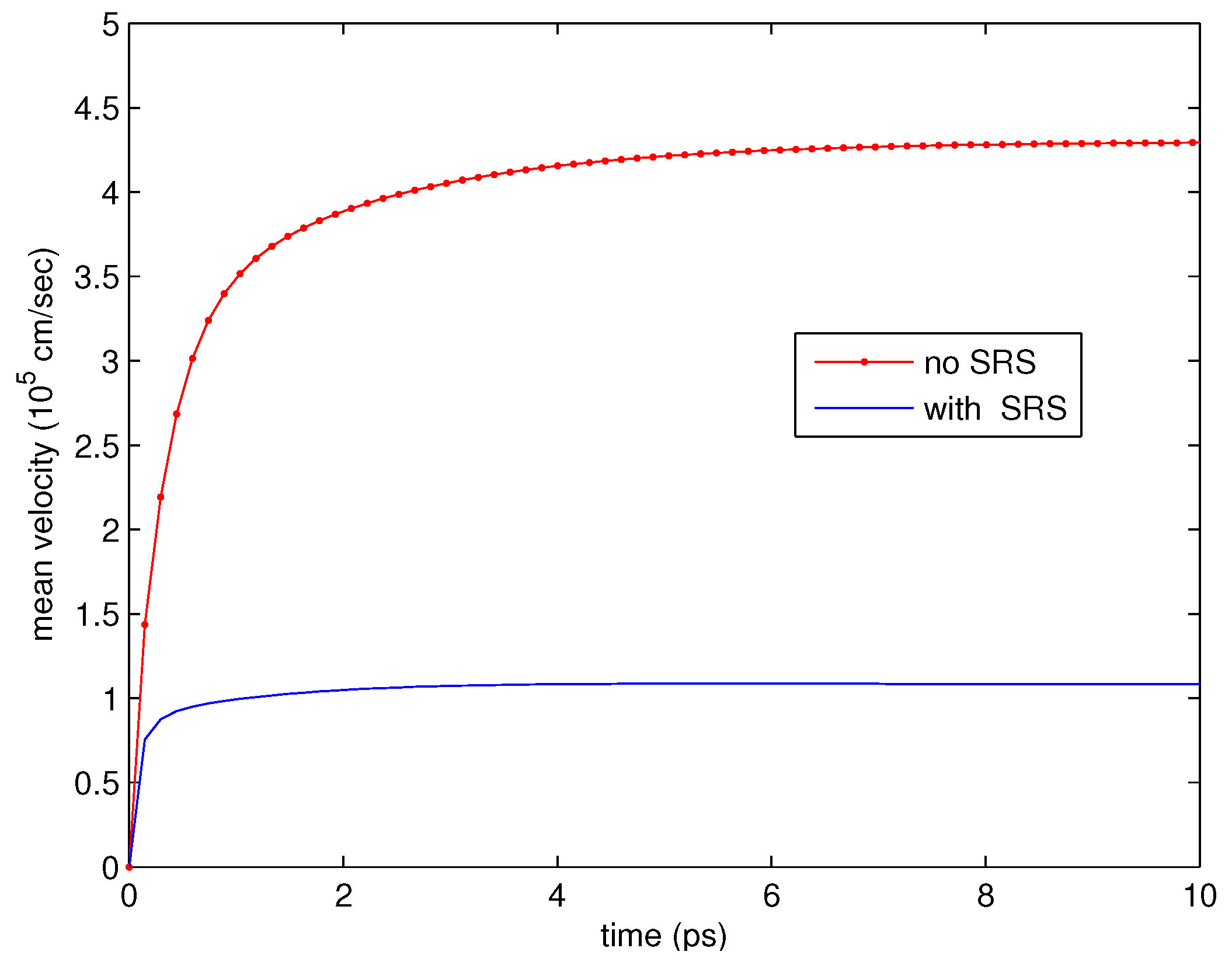
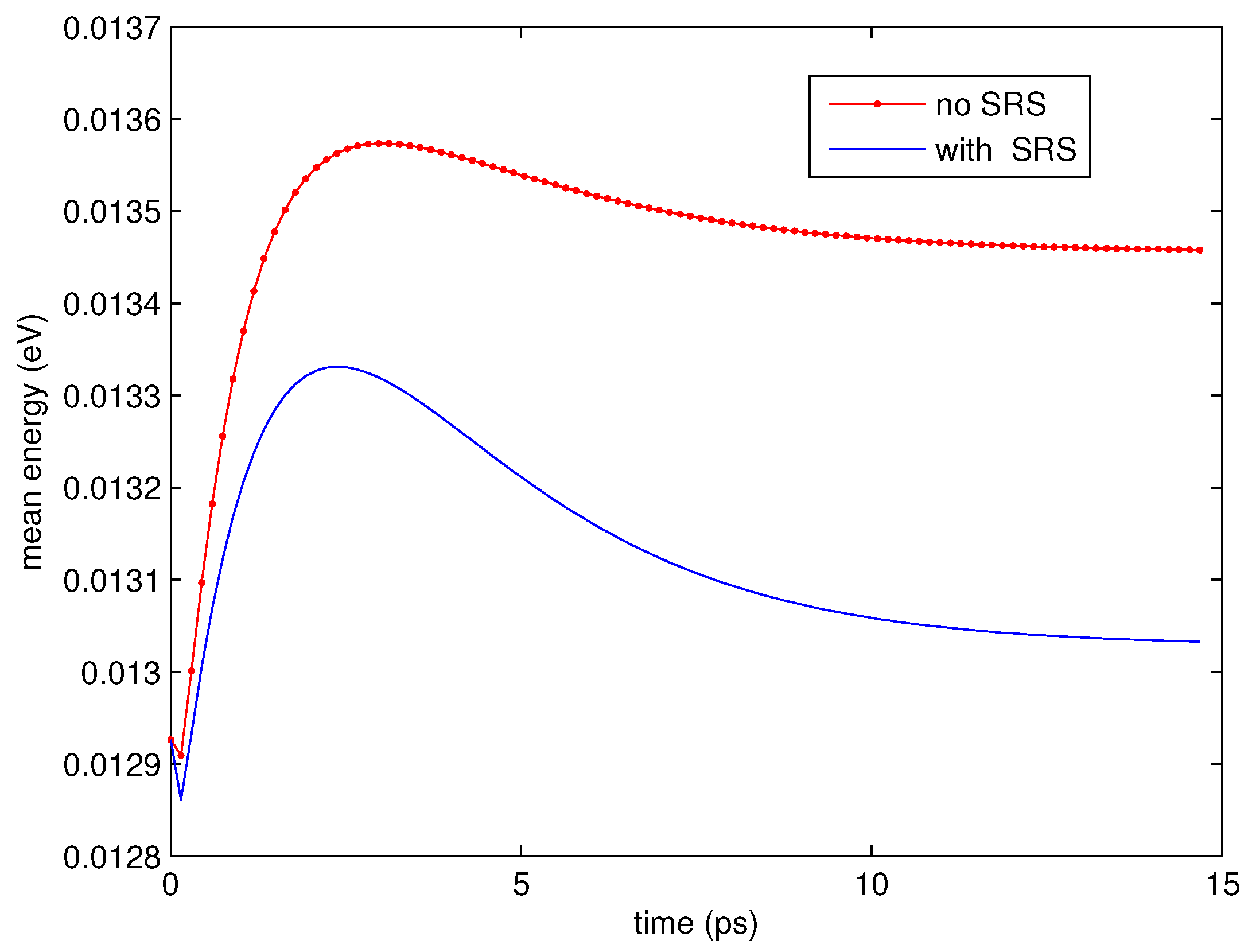
In
Figure 6,
Figure 7 and
Figure 8, we show the mean velocity (40), energy (41) and energy-flux (42), respectively, versus the simulation time, obtained with and without the SRS mechanism. In these figures, one observes that the stationary regime is reached in a few picoseconds for the velocity and the energy flux, in about ten picoseconds for the energy, and the dependence on the SRS mechanism is clearly understood.
Finally, we have computed the low-field mobility
, which is a fundamental parameter for engineering applications. It is defined as the ratio between the average electron velocity, evaluated in the stationary regime, and the driving field (
1 kV/cm), i.e.,
where
are the mobilities in the respective valleys.
In
Table 2, the results for the
A and
B valley mobility, obtained with and without the SRS mechanism, are presented. The difference between these values proves that the SRS is a key mechanism in the SiNW device performance. In the above table, we can notice that mobility in the
A-valley is bigger with respect to that obtained in the
B-valley. Since the mobility depends (inversely) on the effective mass, the valley splitting reduces the mobility along the axis of the wire (in the
B-valley where the effective mass is 0.94), but quantum confinement increases mobility in the transverse direction (in the
A-valley where the effective mass is 0.27).


