1. Introduction
Matrix arithmetic is usually the core computation of complex signal processing algorithms [
1]. Digital images are stored in matrix format, and then, any filtering, modification, decision, or recognition needs matrix algebra. In complex neural network algorithms, the weights are presented in matrix format, and the inputs are multiplied by a matrix of weights [
2]. Adaptive filters in control systems such as Kalman filters need matrix algebra. Many other fields such as navigation systems, wireless communication systems, or graph theory, among others, have also a great deal of matrices.
Numerous scalable implementations of dense matrix-by-matrix multiplication [
3,
4,
5] and dense vector-matrix multiplication [
6] exist. However, most of them use external memories to save input matrices and then extra FIFOs to fetch matrix elements from memories, requiring extra registers to save temporary results [
7,
8]. This usually increases latency and power consumption. An approach for dense matrix-matrix multiplication based on circulant matrices was proposed in [
9], allowing matrix multiplication time to be
without any FIFO and internal registers required to prefetch matrix elements and save temporary results.
In some cases, flexible architecture proposals go beyond multiplication, permitting different matrix operations [
10]. Some of these Matrix Computing (MC) architectures have been targeted toward applications such as big data [
11] or polynomial matrix multiplications [
12]. In some cases, matrix computation parallelization is targeted at multiprocessor systems [
13].
However, the matrix computation architectures proposed to date are aimed mainly at the performance of a single matrix operation, failing to optimize the data flow for a sequence of operations. Note that, generally, the result of matrix-based digital signal processing algorithms relies on a sequence of matrix operations (e.g., multiplication, then addition, then subtraction, transpose, etc.), where intermediate results are used as the operand for a new matrix operation again and again, until the end of the computation (see
Section 3 for an example case). To address a sequence of operations, matrix computing architectures generally need moving data from the intermediate result matrix to the input operand memory in order to be able to undertake the following operation of the sequence. Additionally, a more serious drawback appears when the result of a matrix operation must be sent to external memory to be used as the operand for the next matrix operation. In these cases, a serious overhead appears when considering the complete sequence of matrix operations. Thus, to optimize the performance of computing a sequence of matrix operations, the data flow is as important as optimizing the performance of each matrix operation individually.
This work aims to design a matrix-computing unit on the basis of a circulant matrix multiplication architecture, allowing one to preserve the efficiency of the circulant matrix multiplication while extending it to other operations and optimizing the data flow to compute a sequence of matrix operations. There exists an extensive literature about the use of GPUs for matrix operations. Despite the proposed architecture improving many proposals running on GPUs, this work is not intended to serve as an alternative to GPU computing. The use of a GPU requires high power and a desktop computer, while a single-chip FPGA solution offers low power and small size, with applications in many different fields where small and portable devices are required.
This work aims to design a matrix-computing unit taking advantage of the efficiency of the circulant matrix multiplication [
9] while extending it to other operations and optimizing the data flow to compute a sequence of matrix operations. The main contributions of this paper are as follows:
We propose a universal square matrix-computing unit, based on a circulant matrix structure. It computes matrix-by-matrix, matrix-by-vector, vector-by-matrix, and scalar-by-matrix operations in the same hardware. This architecture is able to compute multiplication, addition, subtraction, and dot product.
The proposed matrix-computing unit is scalable. It has been designed for square matrices of arbitrary size, the maximum matrix size only limited by the available memory in the device.
The proposed architecture shows a great data flow optimization. The results of a matrix operation are available as input for the next matrix operation without data movement, avoiding delays and reducing clock cycles.
The proposed architecture is able to perform arithmetic operations in direct or transposed forms by a simple modification in the addressing of the memory; it can be thought of as an immediate execution of the transpose operation without delay penalty.
We propose an FPGA-based implementation of the matrix-computing unit. It is a flexible FPGA core, reusable for performing complex algorithms.
We develop a graphical user design tool to assist the user in defining a customized matrix computation core IP according to his/her needs.
Despite that the proposed matrix computation architecture can be implemented in VLSIor FPGA, increasing the capacity and reconfigurability of Field Programmable Gate Arrays (FPGA) makes these devices the best candidates to implement high-throughput and complex signal processing algorithms quickly. The large number of high-speed I/O pins, local memories, and DSP blocks enable FPGA to perform fast massive parallel processing. In addition, FPGA are more efficient in power consumption and processing speed than general-purpose processors, and VLSI is the option for high-volume production. With such characteristics and the ubiquity of the matrix-based digital signal processing algorithms, FPGA devices have become a usual platform for fast matrix processing architectures.
This paper is organized as follows. The circulant matrix multiplication process is described in
Section 2.
Section 3 describes the proposed arithmetic algorithms for different matrix operations, using a circulant matrix architecture.
Section 4 discusses the proposed hardware architecture, and
Section 5 describes the developed SCUMO (Scalable Computing Unit for Matrix Operations) design user interface. Implementation results and discussion occupy
Section 6, and
Section 7 concludes the work.
2. Circulant Matrices and Matrix Multiplication
The proposed matrix-computing unit is built on the basis of circulant matrices to compute matrix operations efficiently. This section describes the multiplication process as the basis for the rest of the computations.
Consider two
matrices
P and
G. The multiplication result
is an
matrix. Elements of
R are computed according to Equation (
1).
Then, the first column of the resulting matrix can be computed as shown in Equation (
2).
Let
and
denote vectors containing the
column of the
P and
R matrices and
and
represent vectors containing the
row of the
P and
R matrices. Equation (
2) can be rewritten as in Equation (
3).
This formulation changes the vector-by-vector multiplication operation to a summation of vector-by-scalar operations, which is simpler to compute in hardware. The extension to all columns of the
R matrix is described in Equation (
4).
This approach can be used for different matrix multiplication possibilities, as shown in
Table 1, by changing the computation indices. Note that, in all cases, computation is made by a cycle of scalar-by-vector operations.
To compute all possible states of multiplication of two input matrices, it is necessary to access all elements of the
and
vectors at the same time. In conventional methods, the main problem concerns the matrix elements’ access, typically stored in a memory where it is not possible to access all elements of
simultaneously. To overcome this problem, the circulant matrix structure is used [
9]. The circulant form of an
matrix is a matrix whose elements in each row are rotated to right one element relative to the preceding row [
14]. Equation (
5) represents an
matrix in circulant form, and
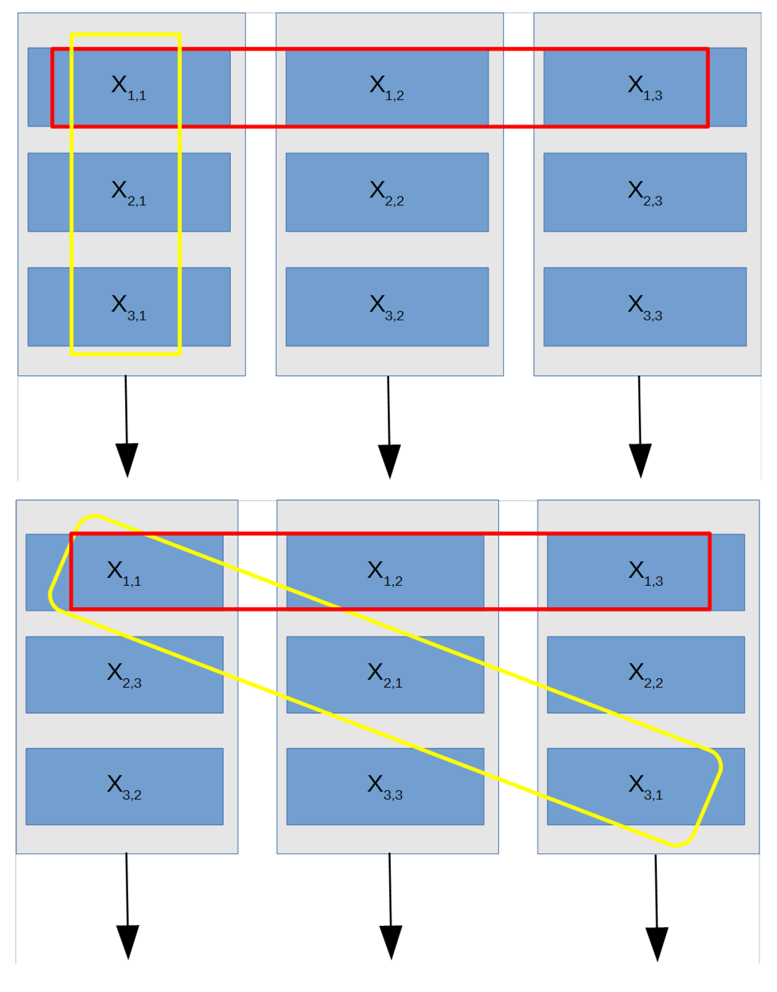
Figure 1 shows the physical memory locations for
matrix elements in normal and circulant forms.
An optimal matrix elements’ storage is possible by obtaining the circulant matrix and storing each of the obtained columns in a different RAM memory, thus requiring N memory blocks
. As seen in
Figure 1, the elements of each column or row vector are saved in different memory blocks, and all elements of each row or column are simultaneously accessible since these memory blocks are fully independent of read or write. The read address of the elements of a column vector
i in different memory blocks can be written as
, where
is the address of the element in the first memory and
i the read address in the next memory block
. Thus, we can produce one address for the element in the first memory, and then, the addresses for the other columns can be computed from that initial address. Therefore, by incorporating an internal address increment for that address according to the memory block position, only one address bus is required for all memory blocks, greatly reducing the interconnection lines and, thus, reducing the resource usage. For instance, accessing all elements in column
from
Figure 1 means that each memory block must read values in Addresses
from memories
,
,
, respectively. Thus, a complete matrix column can be read in a single clock cycle, ready to be multiplied by an scalar value.
An additional advantage of matrix memory storage as a circulant matrix lies in the fact that the transpose matrix can be read by changing the addressing order, i.e., a matrix row can be simultaneously read in a single clock cycle. In the general case of a matrix
X as shown in
Figure 1, an
row can be accessed by reading from the same address location in all memory blocks, i.e.,
. As an example, reading
requires accessing Address 1 in all memory blocks. This form of access to elements in row or column form is selected in each block from an external line, as explained in
Section 4.
This scheme can be efficiently implemented in hardware for matrix element access by using modulo N counters. In case of matrix operations, we assume that one matrix (e.g., P) is stored in RAM memories in circulant form and the other matrix (G) is externally fed, assuming that a single value from G is entered into the computation system every clock cycle. As explained earlier, all operations are converted to vector-by-scalar operations, and thus, operating with matrices P and G means that P row or columns are simultaneously accessed and individual G values are serially entered into the architecture.
Once the partial row or column computation result is obtained, it must be internally stored. This is done in the existing RAM memories by defining each RAM memory to be in size. Then, one half of the memory stores one column operand from P, and the second half stores the vector-by-scalar computation result. After completing the process, the second half of the memory contains the matrix result, which is ready to be used as a matrix operand in the next operation by switching the read address to the second half and storing the new result in the first half. Alternating this memory paging method, no delay penalty between successive matrix operations exists.
Let us explain the multiplication process of two
matrices
P and
G. The product
is computed by addressing
P values beginning from
down to zero for the first row,
down to (
) for the second row, and zero down to (
) for the
row, i.e., one element for each RAM memory is read. Once all
P values are simultaneously read, they must be multiplied by the same
G matrix element, as shown earlier. This is achieved by including
N arithmetic units (referred to as ALU), which multiply each
P value by the
G value in a concurrent form to obtain all partial products described in Equation (
4). Lastly, the addition of the partial products generates the final result.
To illustrate the process, the computing algorithm for the first column of
for
matrices is presented in Algorithm 1. This algorithm performs all required computations described in Equation (
3) for
. It is assumed that
and
are row and column addresses of the required
G matrix element, which are externally fed in its corresponding order. Three ALU units are included to compute parallel multiplications, and
P matrix elements are stored in circulant form, distributed in the RAM memories according to the addresses indicated in
Table 2.
| Algorithm 1 Sequence of operations for matrix multiplication (). By using concurrent arithmetic operations, one column result can be obtained after three clock cycles (Ncycles for the general case). The complete computation result is achieved in cycles for matrices. |
| | ▹ |
| |
| |
| |
| |
| |
| |
| |
| | ▹ |
| |
| |
| |
| |
| |
| |
| |
| | ▹ |
| |
| |
| |
| |
| |
| |
| |
After three clock cycles (one round), data are saved in memory, and the computation of the second column starts. In three rounds, all R elements of the resulting matrix are obtained by shifting partial products between columns in a ring from left to right. In the general case, an multiplication is obtained after clock cycles. The resulting elements of matrix R are stored in the unused area of memory blocks (second half of the memory block) in circulant form, which allows its use in further matrix operations, e.g., multiplication of matrix R by a new matrix externally fed into the system.
3. Matrix Computing Unit Proposal
The architecture of the proposed matrix-computing unit has been designed to optimize both the performance and the data flow of the complete sequence of matrix operations. To do that, an extension of the circulant matrix multiplication architecture [
9] is proposed. This architecture permits keeping the matrix multiplication computationally efficient and, at the same time, exploiting some relevant data flow benefits to improve the performance of the whole computation sequence:
- -
Instant transpose operation (zero overhead for transpose): The matrix stored in the unit can be used as an operand in direct or transposed form by a simple modification in the addressing. This is done without data movement. Thus, transpose operation can be thought of as an instantaneous operation.
- -
No data movement between operations (internal intermediate storage): The unit contains a temporary matrix storage. This is done by doubling the size of RAM memory blocks where the result of the operation is stored in circulant form, ready to be used as one of the matrix operations in the next operation. This mechanism enables chaining matrix operations, avoiding the need of writing intermediate results in a memory out of the unit before the end of the sequence, preventing delay penalties of data movements.
Together with matrix multiplication, the proposed computational architecture allows the following operations: matrix addition, matrix subtraction, matrix dot product, and scalar-by-matrix multiplication. In all cases, it is possible to choose if the internal matrix uses its direct or transposed form for the next operation. Algorithm 2 illustrates a case example computed by the proposed unit. As seen in the algorithm, no extra time for new computations is required since a continuous data feed is done while computing.
| Algorithm 2 Use of the proposed matrix-computing unit to solve an example matrix expression. The sequence of matrix operations required to achieve the final result is shown. |
| Example expression: |
|
| Step 1: | Load matrix () into the unit. |
| | Load coefficients of matrixinto the unit. |
| | |
| Step 2: | Multiplication () with the inner matrix. |
| | Loadcoefficients while computing |
| | Resultingmatrix stays inside the unit when finished. |
| | |
| Step 3: | Multiplication () with the (transpose) inner matrix. |
| | Address control signals to read inneras the transpose. |
| | Loadcoefficients while computing |
| | No overhead cycles spent to transpose the inner matrix. |
| | Resultingmatrix stays inside the unit when finished. |
| | |
| Step 4: | Add () with the inner matrix. |
| | Loadcoefficients while computing |
| | Resultingmatrix stays inside the unit when finished. |
| | |
| Step 5: | Scalar (k) by (transpose) inner matrix multiplication. |
| | Address control signals to read inneras the transpose. |
| | Computes input scalar k by inner matrix multiplication. |
| | No overhead cycles spent to transpose the inner matrix. |
| | Resulting |
| | stays inside the unit when finished. |
| | |
| Step 6: | Operation: Read inner matrix (computation result). |
| | Resulting matrix coefficients are read from the unit. |
Matrix multiplication was described in
Section 2. Let us describe how the same hardware architecture can serve to compute other matrix computations.
3.1. Transpose Matrix
Algorithms 3 and 4 show the cases of address generation for and , respectively. Indices k and l are iterations, and and are the row and column addresses of the required G matrix element. For direct matrix multiplication, a circulant addressing mode is used, and matrix elements are read column-wise. In transpose mode, normal addressing mode is used, and matrix elements are read row-wise. In case of multiplication by a transposed matrix , and addresses should be swapped. The row addresses become column address, and vice versa. As can be seen, obtaining the direct or transposed only form requires a different reading order of P elements.
Thus, it is not necessary for the core to be able to compute all operations, because after loading the G matrix in the internal memory, the result can be computed in the same form as , but only changing, through control signals, how the elements of the internal matrix are read to operate (e.g., in direct or transpose form). This ability has been added to increase the flexibility of the system. d to operate with (e.g., in direct or transpose form). This ability has been added to increase the flexibility of the system.
| Algorithm 3 Addressing scheme for computation. |
| |
| |
| for k=1:N do | |
| for l=1:N do | |
| | |
| | |
| | |
| | ▹ |
| end for | |
| end for | |
| Algorithm 4 Addressing scheme for computation. |
| |
| |
| for k=1:N do | |
| for l=1:N do | |
| | |
| | |
| | |
| | ▹ |
| end for | |
| end for | |
This flexibility can be used to adapt the computations. Based on matrix-by-matrix multiplication properties, some equivalences as shown in Equation (
6) can be done. To compute these multiplications, one may prefer to use its transposed form in the operation and then compute the transpose of the result. An interesting property in the circulant form of a matrix is that both
and
elements are stored in the same memory column. By changing the writing address from circulant form to normal form (
), the transposed operation is controlled. For example,
computation using
offers the same result as computing
using
.
3.2. Matrix Addition, Subtraction, and Dot Product Operation
Matrix addition, subtraction, and dot product operations share the same algorithm for address generation. The only difference lies in the operation, which must be set to add, subtract, or multiply, accordingly. These operations require arithmetic operations. Algorithm 5 shows the addressing scheme for these operations. Input signal controls the write operation into memories. Based on the transpose property of a circulant form of the matrix, only the input should be set to zero. For the addition or dot product with the operand, the values of and must be swapped.
| Algorithm 5 Addressing scheme for and computation. |
| |
| |
| for k=1:N do | |
| for l=1:N do | |
| | |
| | |
| | |
| | |
| | ▹ |
| end for | |
| end for | |
3.3. Scalar-by-Matrix and Vector-by-Matrix Multiplication
To perform the scalar-by-matrix multiplication, we have two possible operations for a given scalar S and an matrix: and . It performs in N clock cycles. For each clock cycle, all the elements of one row will be multiplied by S. Algorithm 6 shows the addressing scheme for computation. To compute , the input must be set to one.
| Algorithm 6 Addressing scheme for computation. |
| |
| |
| for k=1:N do | |
| | |
| | ▹ |
| end for | |
For the multiplication of an matrix P by an vector V, two operations are possible: and . The algorithm computing and is similar to Algorithms 3 and 4, respectively. The difference is that for both algorithms. For the multiplication of an vector V by an matrix P, we also have two operations: and . The algorithm computing and is similar to Algorithms 4 and 3, respectively. In this case, for both algorithms, the value for and should be swapped, and .
4. Hardware Architecture for the Matrix Computation Core
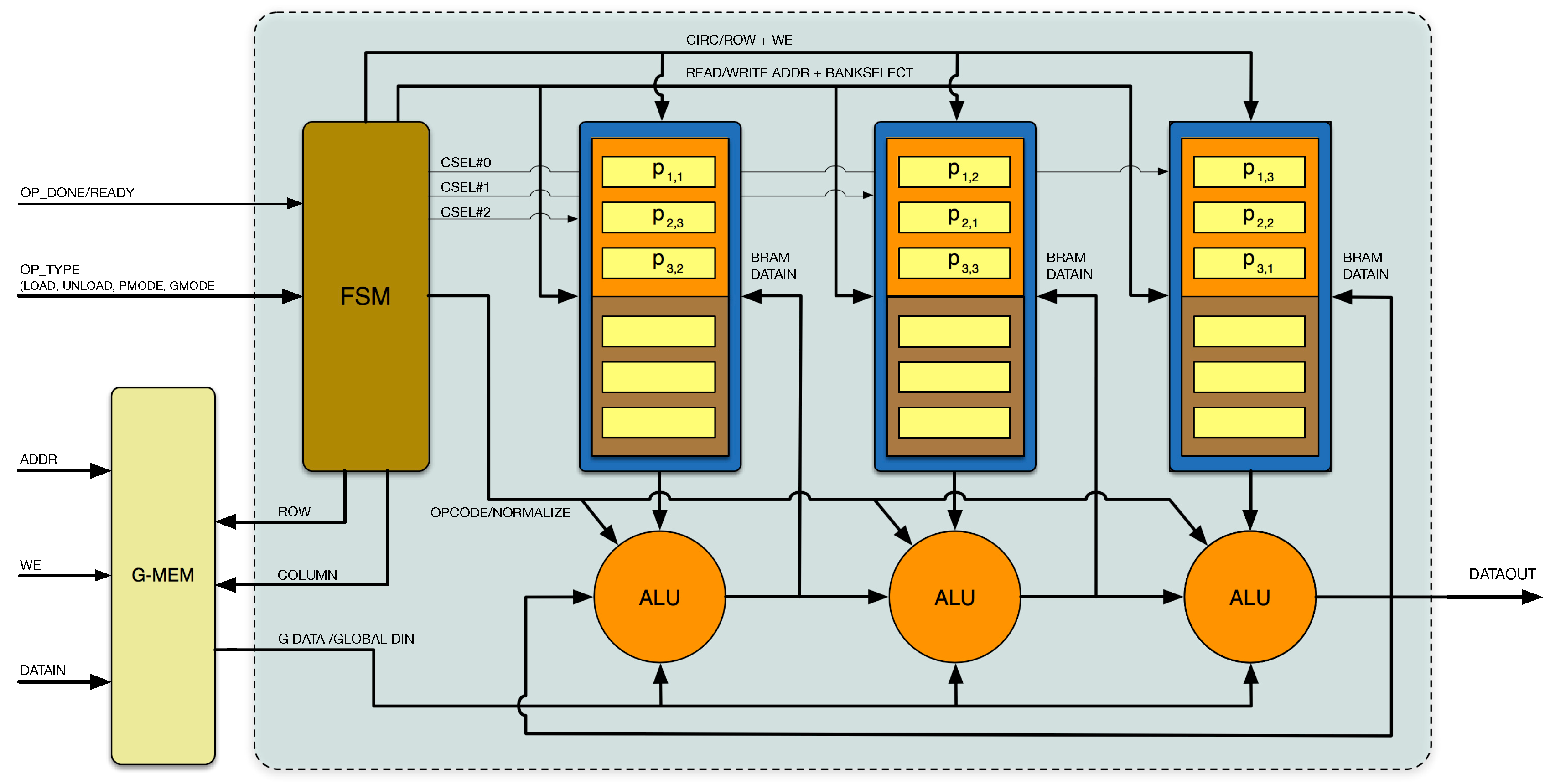
The proposed hardware architecture supporting all aforementioned matrix operations is presented in
Figure 2. It consists of a systolic ring of ALU-RAM blocks containing two parts: a memory block and an arithmetic unit. Each
P matrix column is stored in circulant form, and the Finite State Machine (FSM) block receives external configuration modes and controls the data flow: address generation, data shifting, synchronization of control signals to modules, etc.
For the general case, an matrix requires N memory blocks and N ALUs in order to assess all elements in clock cycles. It is important to note that elements are calculated by successive shift-multiply-add operations, passing intermediate results in a ring from left to right.
To operate, it is always assumed that one matrix (referred o as P) is internally stored in the memory blocks in circulant form, and the second operand matrix (G), vector (V), or scalar (S) is stored in an external memory, or externally fed by another hardware, upon issuance of the required address (from the FSM by and signals). The proposed architecture uses the port to feed , and S data, but also for data loading through the ALU, so that new matrix data values can be stored in RAM to act as the P operand. The main principles used in this architecture are the locality of the computation and the use of global control signals to reduce delays and optimize logic resources.
The FSM is controlled by the user via a 5-bit data bus () indicating the desired operation to the computing unit (load, unload, or arithmetic operation to be performed). After that, the FSM generates: a sequence of control signals etc.; the addresses and control signals for the systolic ring; and signals; and determines the operation of the ALU blocks. The user can write the operand on the fly, as long as a constant write latency is guaranteed.
The FSM block is fully modular to decrease the complexity of address generation. It consists of five sub-blocks to generate address and control signals for different operations. These sub-blocks are: loading, unloading, multiplication, addition (also valid for subtraction), and scalar multiplication. By using the modular approach, new functionalities can be added without modification of the existing hardware. The multiplication sub-block controls both matrix-by-matrix and matrix-by-vector multiplication. The addition sub-block controls addition, subtraction, and dot product operations. The rest of the sub-blocks are used for a single operation.
The data comprise a 3-bit bus containing , , and signals going to memory blocks. As the input matrix P and the results are saved in the same memory block, the signal determines if the P matrix elements are in the upper bank or lower bank of the memory block (alternatively, P data are in the upper block, while R data in the lower block, or vice versa). There are N signals, which enable or disable the read/write of memory blocks. All ALU blocks share the signal, which enables normalization of the multiplication results based on fixed point arithmetic. It is important to note that signals are the only specific signals of the ALU-RAM blocks; all the others are common bus signals. This property eases routing problems as a reduced number of interconnection lines is required. Moreover, there is no multiplexing in data and address paths, which reduces delays and increases the maximum possible frequency of the system. After finishing the selected operation, the FSM raises the signal high, and the user can offload resulting data from the core or start a new operation.
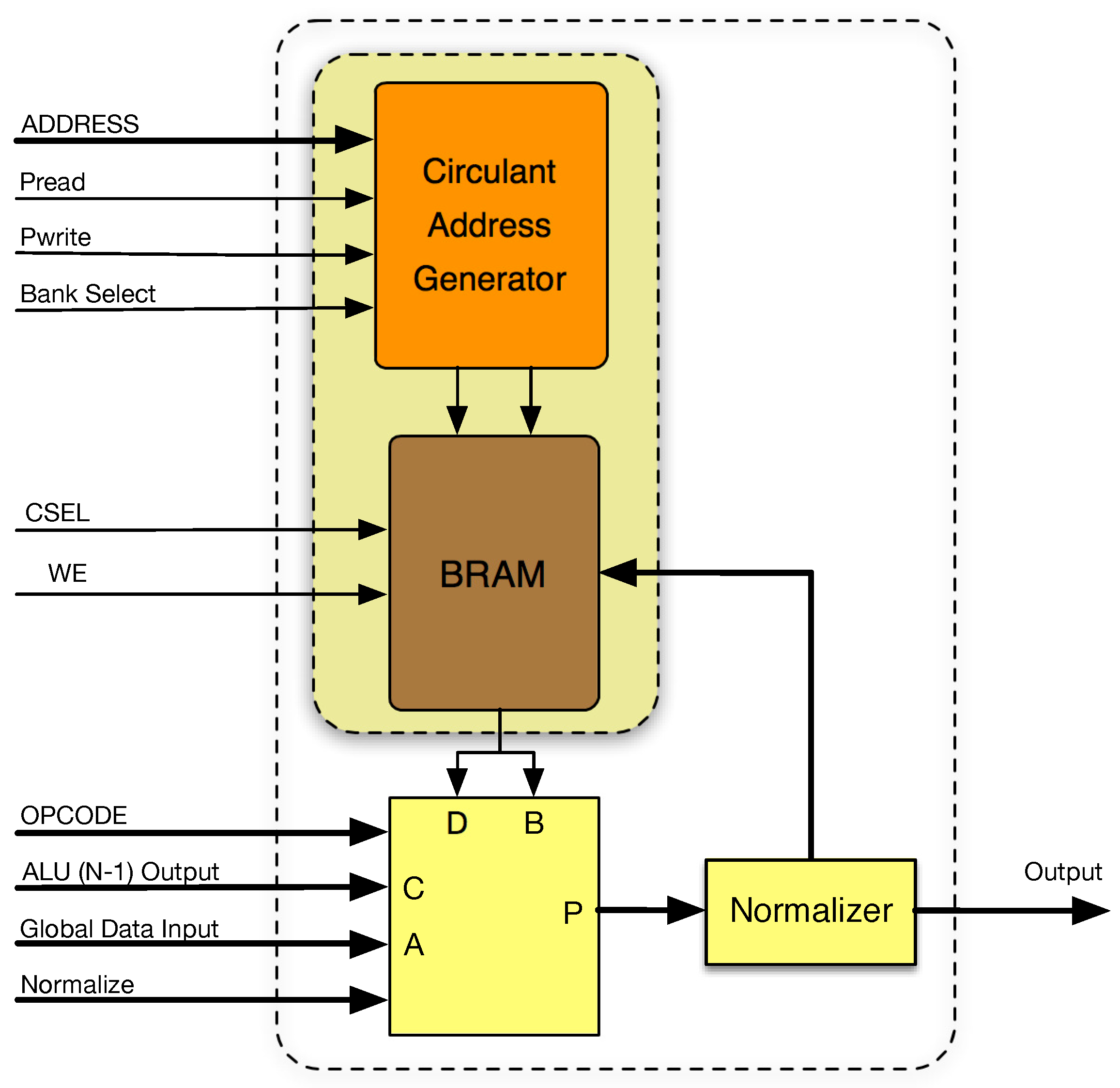
Figure 3 shows the internal architecture of the proposed ALU-RAM column architecture. A true dual-port memory block primitive must be used to store the
P operand and the resulting
R matrix elements with independent data in and data out ports. Thus, its size must be
, at least. In addition to the memory, an additional logic element is required: the module “circulant address generator”. It is based on the received address from the FSM and the mode of operation (direct or transpose) and calculates the physical memory address to be read as described in previous sections. Finally, the ALU-RAM block includes an ALU able to perform
, where
P is the ALU output,
A is the global data input, and
B and
D are connected to the output port of the memory block. Input
C is connected to the ALU output of the adjacent ALU-RAM block on the left, serving as a propagation line of the systolic ring. In the same way, the output of each ALU-RAM block is connected to the input
C of the adjacent ALU-RAM block on the right (chaining thus ALU-RAM blocks), as well as to the RAM data input port, for memory storage.
Once defined, the architecture was coded in the VHDL hardware description language. When coding, the main aim was to define a versatile, parameterizable and synthesizable code accepting all possible architecture possibilities, such as matrix size or data bit-length. The resulting code is synthesizable in any FPGA device; the optimal implementation was done in those FPGA devices including RAM Blocks (usually referred to as BRAM) and ALU blocks (usually referred as DSP blocks). In this case, the best performance and resource usage can be expected. Despite its generality, Xilinx FPGA was used for this implementation.
5. SCUMO Software Design Tool
There is general agreement that software is now a dominant part of the embedded design process. Digital circuits are becoming more complex, while time-to-market windows are shrinking. Designers cannot keep up with the advancements in engineering unless they adopt a more methodological process for the design of digital circuits. For this reason, according to computational intelligence paradigms, CAD tools are required to take advantage of the technological advances and provide added value to embedded systems so that the design cycle can be shortened, to be competitive in the market and to accelerate their use by multiple users. Actually, the use of CAD tools supporting complex hardware design systems is not new in hardware/software codesign [
15,
16] and software applications. It supports the design and configuration of custom hardware implementations [
17,
18,
19].
As the proposed matrix computation core allows multiple configuration possibilities, a CAD tool with a graphical user interface based on MATLAB has been developed. This tool, called SCUMO (Scalable Computing Unit for Matrix Operations), allows introducing configuration parameters, automatically generating hardware description code (VHDL) for FPGA implementation, and also creating hardware test benches for design verification. Thus, the generated code is ready to be used by the FPGA commercial tool provided by the device manufacturer for final implementation and simulation. SCUMO controls the FPGA implementation tool in the background, launching the process and collecting resulting data to be displayed in the user interface.
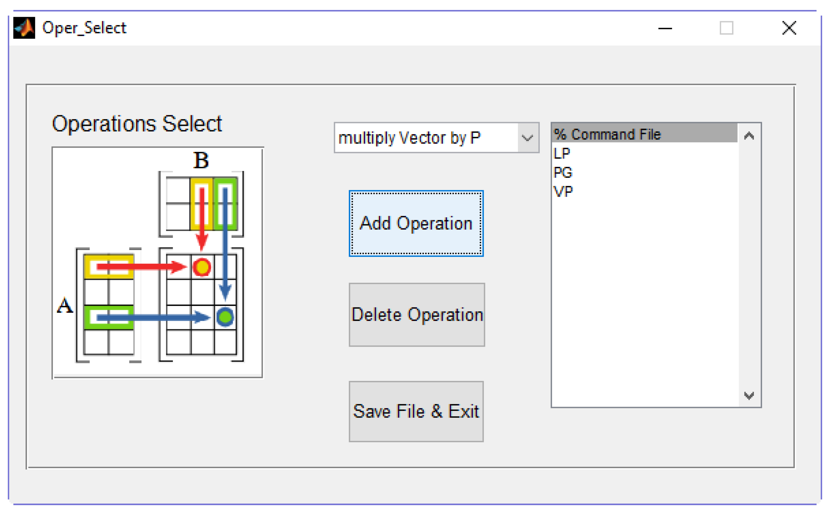
The first step in the use of SCUMO consists of the user introduction of the desired arithmetic matrix operations to be performed by the core. All arithmetic operations are given in a box, and the user must choose among them. A total of eight arithmetic operations is offered. After selecting all configuration options, the software tool creates the implementation code and test bench; then, the FPGA synthesis process is launched (background execution of proprietary Xilinx FPGA tools). Finally, synthesis results are collected and shown in the software to show all relevant information about the implementation process in the SCUMO user interface.
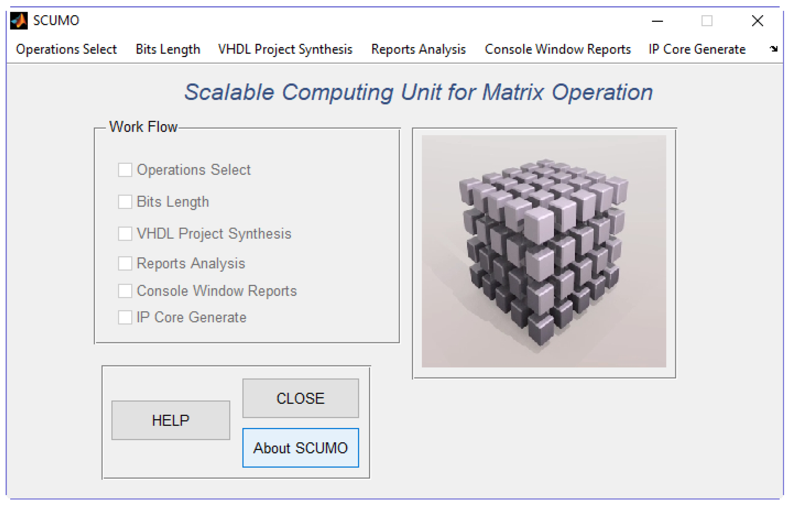
Figure 4 shows the main user screen where the work flow (“Work Flow Panel”) is indicated by tick marks. This panel informs the user about the completion of the different required steps leading to hardware implementation. Additionally, the panel assists in following the proper order of execution, since the work flow must be executed following a strict order (otherwise, a message box informs the user). While one of the steps is being executed, a wait bar appears to inform the user that no other actions can be executed.
Six actions require the user’s intervention to configure the computation core:
Operation selection: The user must select those matrix operations to be executed in the hardware computation core.
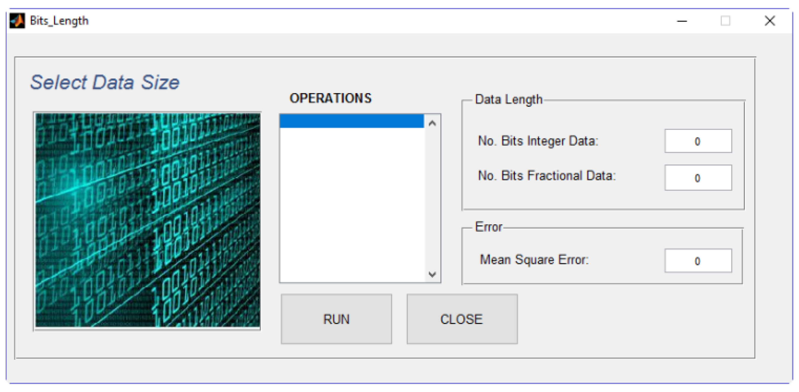
Bit length: The software tool analyzes the selected operations and calculates the optimum bit length in format.
VHDL project synthesis: The user must select one of the FPGA devices offered in a list and synthesis options.
Report analysis: The synthesis process considering all previous configurations is launched.
Console window reports: The synthesis reports are shown to the user.
IP core generate: A wrapping of the core is finally done in order to pack the generated code and make it available for further integration with more complex designs or to be used as a standalone module in an FPGA.
Figure 5 shows the selection list (list box) where the user includes the type of matrix, vector, or scalar operations that are required to be included in the hardware core. Depending on the arithmetic operations chosen, the bit length must be properly selected to avoid overflow problems. For this reason, a specific step is included (
Figure 6) so that the user can upload sample data files including the expected values of
P and
G to be calculated by the hardware core, and the tool will estimate the most adequate bit length for the design (integer and fraction part of the QX.Ydata format type) and the estimated mean squared error that the hardware implementation will have when compared to a PC-based floating point counterpart. Additionally, the introduced data files can be used as a simulation test bench in the hardware design simulation tool (ISE simulator or ModelSim, in this case).
After selection of a specific Xilinx FPGA device, the “VHDL Project Synthesis” option launches the Xilinx synthesis tool by using tcl/tkcommands, which allow one to inform the synthesis tool about all selected parameters required to carry out the synthesis of the core.
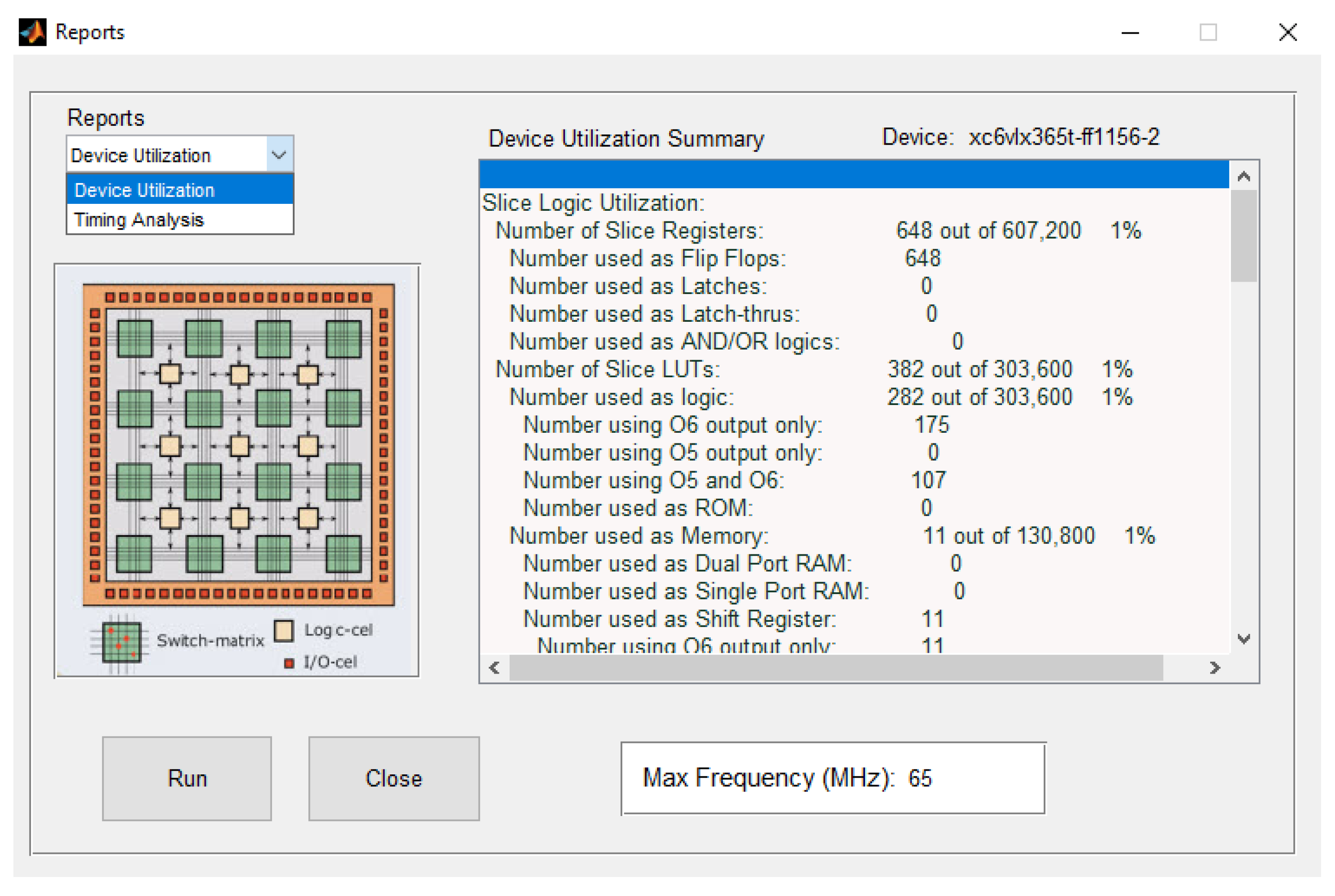
The “Reports Analysis” option shown in
Figure 7 deploys all related information after the end of the synthesis process. A list box allows the user to navigate through timing analysis and device utilization information collected from all the synthesis tool-generated information, including the maximum clock frequency of operation.
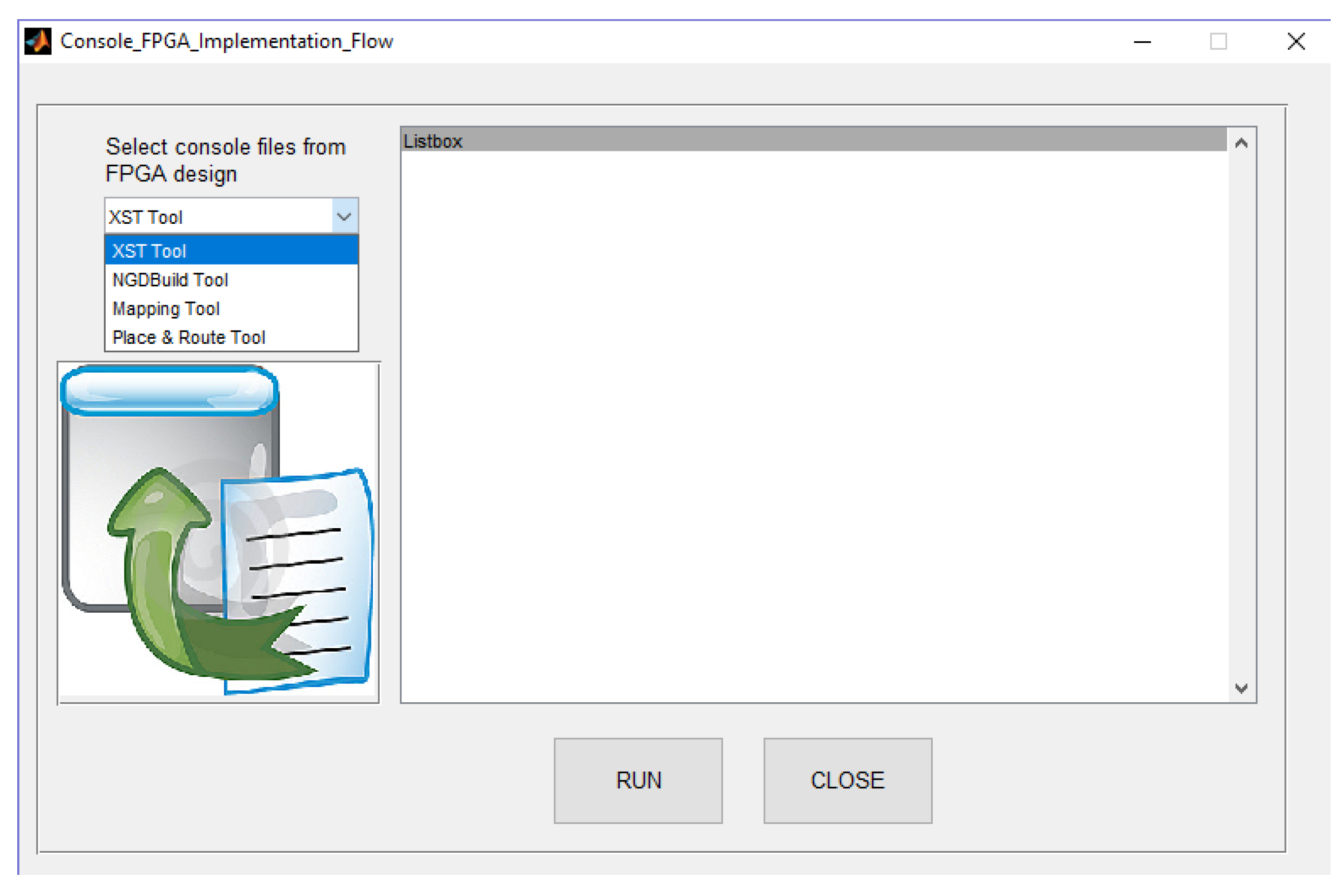
The user can obtain further detailed information in the “Console Window Reports” option (
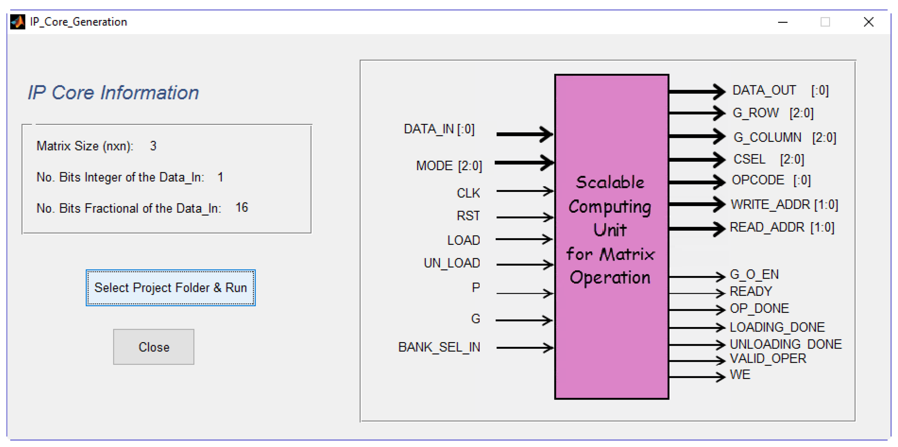
Figure 8) where more detailed translate, mapping, and place and route information can be obtained. At last, the hardware computation core can be generated by selecting the “IP core generate” option (
Figure 9). All parameters and interfacing signals are included in the created files, ready to use as part of bigger designs or standalone computing device.
6. Implementation Results
In order to analyze the proposed architecture, the selected design in the SCUMO software used the XC7VX485TFFG1157 Xilinx Virtex 7 FPGA device with 18-bit fixed-point precision (QX.Y format where X + Y = 18). The obtained system was tested using Xilinx ISE 14.2.
In this design, the DSP48E primitives were used as the ALU block described above. Each one of these high performance block is an arithmetic block containing a 48-bit pre-adder, a
multiplier, and a 48-bit MAC-adder.
Table 3 shows the required resources and maximum available clock frequency for five different matrix sizes. As seen, the number of DSP48E and block RAM slices was directly related to matrix size. Selecting more than 18 bits doubled the need for DSP slices and increased the amount of necessary logic.
The last row in
Table 3 (referred to as “Slices vs. Size”) shows the ratio between the number of logic resources (slices) and the matrix size. It can be observed that this ratio was relatively constant for different matrix sizes, which means that no extra logic was generated when matrix size increased.
Concerning the maximum clock frequency of operation, in the case of a matrix, a clock speed of 346 MHz was achieved, which means an overall performance of 173 GOPS since 500 operations were being executed at every clock cycle. The maximum clock frequency decreased with the matrix size due to some long delay lines. However, the frequency decrease ratio was low when compared to the matrix size increment: 404.4 MHz and 346.1 MHz was obtained for matrix size of 10 and 500, respectively.
Table 4 shows the number of clock cycles necessary for different operations of the matrix- computing unit. As is shown, matrix-by-matrix multiplication, addition, subtraction, dot product, vector-by-matrix, and scalar-by-matrix multiplications were performed in
clock cycles. It is important to note that the global core latency was only seven clock cycles, regardless of matrix size. This latency comes from the following sources:
- -
One clock cycle at the sequential arithmetic sub-units in the DSP block.
- -
One clock cycle at the addition operation.
- -
One clock cycle at the multiplication operation.
- -
Two clock cycles at the outputs of BRAM memories.
- -
Two clock cycles at the FSM unit.
While the latency issue can be important for small matrices, the delay of seven clock cycles became negligible for large sizes.
Something similar arose for loading (storing matrix values in RAM blocks) and unloading (reading matrix values in RAM blocks) operations, requiring
and
clock cycles for completion, respectively. In addition,
Table 4 shows the peak frequency at which the unit can repeatedly perform each operation (considering the required number of cycles and the maximum frequency of operations for each matrix size).
From the obtained results, it can be determined that the proposed matrix computing architecture extended the circulant matrix multiplication architecture [
9] to other operations while keeping the architecture benefits: exploiting local interconnections, data storage, and computations to reduce delays and communication overhead. This fact avoids typical communication bottlenecks in a classical fully-parallel system.
The extension of additional matrix operation performed by the architecture did not affect the matrix multiplication performance, having 173 GOPS of overall performance when computing
matrices. Moreover, the proposed architecture can be a competitor for Graphic Processing Units (GPU) when the matrix size is <1000. In the bibliography, GPU performance ranged from 26.4 [
20] to 350 GFLOPS [
21], but this performance was greatly reduced for intermediate matrix sizes, as in [
21], where performance dropped from 350 GFLOPS to under 50 GFLOPS when the matrix size was <1000. Besides, the circulant matrix multiplication had better performance than the rest of the FPGA-based approaches operating with matrix sizes
, as [
22], who claimed the fastest result for
matrix multiplications. However, the circulant architecture overcame (see
Table 4) this performance by various orders of magnitude. Other implementations for
matrix size are hardly comparable because they tended to use
processing elements [
23,
24,
25].
There exist numerous references dealing with the acceleration of individual matrix operations, but very few consider the implementation of a matrix-computing unit integrating successive and different types of matrix operations. In this sense, the most relevant implementation up to date has been carried out by Wang et al. [
10], who included matrix addition, subtraction, dot product, dot division, and matrix multiplication. In this case, Wang obtained, for matrix multiplication, an average performance of 19.1 and 76.8 GFLOPS on the Stratix III and Stratix V platforms, respectively. As the proposed circulant matrix processor performs 173 GOPS, a superior performance can be claimed. Note that this performance is not affected by the configured word-length (except some extra latency cycles when using more than 18 bits, due to its pipelined design). This performance is also higher than the obtained by Wang et al. [
10] for matrix multiplication on an Intel i7 3770K processor running a 64-bit Windows 7 operating system, obtaining an average performance of 117.3 GFLOPS. On the other hand, our proposed matrix processor surpasses all other matrix processor implementations in the bibliography, as [
26] that required 21,970 cycles to compute a
matrix multiplication, while our circulant matrix processor required only 4013 cycles, being more than five-times faster.
The circulant matrix-computing unit extended matrix multiplication with addition, subtraction, dot product, vector-by-matrix, and scalar-by-matrix operations. The performance measures in
Table 4 reveal an optimized performance with low latency on all of them. Other works in the bibliography did not indicate the performance for other operations except matrix multiplication. The operation having a record-breaking performance, making a difference in our circulant matrix-computing unit, was the transpose operation, which we claim to be immediate because it was done by a simple modification in the addressing of the internal matrix. It can be compared with the transpose operation in [
26], requiring 2,813,396 cycles to compute a
matrix multiplication, while our circulant matrix processor instantaneously did it.
Some authors proposed specific matrix multiplication architectures targeting convolutional neural networks [
5]. In this case, they reported 59.7, 87.8, and 64.9 GFLOPS for matrix computations requiring 105.4, 111.9, and 149.5 million multiplications, respectively. Our work reports 173 GOPS for 125 million multiplications (matrix size of 500). A scalable matrix multiplication architecture was proposed in [
22], reporting 12.18 GFLOPS for a
matrix computation, mainly limited by the use of external off-chip RAM memory. Some authors proposed a combined CPU + FPGA architecture where matrix multiplication tasks were shared [
27]; in this case, the architecture can achieve 4.19 GFLOPS for
matrices by means of block-matrix streaming of data between the CPU and FPGA. Considering our proposed architecture, assuming a 300-MHz clock rate for
, a 60-0GOPS performance would be achieved.
Concluding, the obtained results show remarkable benefits of using the proposed circulant matrix-computing unit. It is an efficient and very deterministic matrix processor allowing one to optimize the computation of a complete sequence of matrix operations with a very low latency and clock cycle overhead.
7. Conclusions
In this article, we propose a scalable matrix-computing unit architecture for the computation of sequences of matrix operations. It is motivated by the increasingly central role of signal processing and machine learning algorithms, which require the computation of matrix algebra equations. Works proposed until now have typically focused on accelerating individual matrix operations. We show that it is possible to optimize both the data flow of the sequence of operations and the performance of individual operations using a circulant matrix storage with systolic ring topology. The FPGA hardware implementation shows that the circulant architecture exhibited and a deterministic performance of clock cycles for all matrix-matrix operations. The architecture also permits chain matrix operations without data movement of intermediate results, or even using the transpose matrix of an operand with just a simple address modification. These data flow improvements are fundamental for the performance of the computation in a sequence of matrix operations.
The SCUMO design environment assists in the hardware options configuration, from definition to the generation of the final IP core. This architecture can be successfully implemented for large matrices: matrices only require N ALU-RAM blocks. Currently, sizes of up to could be implemented, and in general, the architecture can be extended up to the limits of the hardware device. The resulting implementation achieves 173 GOPS for the matrices tested, running at 346 MHz.
We plan to improve this architecture including the possibility of choosing floating or fixed point precision and adapting the control unit to handle rectangular matrices. Note that our proposal can adapt to rectangular matrices by just changing the data control sequence. Moreover, it is likely that the circulant matrix architecture will support the inverse matrix architecture, adding it as a new matrix operation.

 ,
, 


