A Novel Synchronization Technique for Wireless Power Transfer Systems


1
Key Laboratory of Control of Power Transmission and Transformation Ministry of Education, Shanghai Jiao Tong University, 800 Dongchuan RD., Shanghai 200240, China
2
College of Electric and Information Engineering, Zhengzhou University of Light Industry, Zhengzhou 450002, China
*
Author to whom correspondence should be addressed.
Electronics 2018, 7(11), 319; https://doi.org/10.3390/electronics7110319
Submission received: 29 September 2018
/
Revised: 2 November 2018
/
Accepted: 6 November 2018
/
Published: 13 November 2018
(This article belongs to the Special Issue Applications of Power Electronics)
Abstract
:Recently, wireless power transfer (WPT) systems with active receivers have been proposed for conduction loss reduction, bidirectional power transfer and efficiency improvement. However, the synchronization of WPT systems is complex in nature with the selection of high operating frequencies. Without proper synchronization, power oscillations appear and the system can become unstable. In this paper, a detailed analysis of different WPT systems is presented and the essence of the synchronization technique is derived as being composed of two functions: independent frequency locking and reference phase calibration. The voltage across the receiver-side compensation capacitor is divided and utilized for frequency locking, whereas the reference phase calibration is realized through software code. The proposed method is effective and easy to implement, with a lower overall cost due to its simplicity. The technique can work effectively at high frequency and withstand large variations of operating frequency, load and mutual inductance. In addition, it can address the synchronization problem of multiple active receiver WPT systems with and without cross coupling among the receiving coils. Theoretical analysis and experimental results validate the proposed technique.

1. Introduction
Wireless power transfer (WPT) techniques can realize energy transmission through coupled coils without the need for physical contact between the transmitter and the receiver [1,2,3]. Considerable efforts are put into the modeling, performance analysis, design and optimization of WPT systems [4,5,6,7,8,9,10]. The operating frequencies of WPT systems can range from kHz to MHz. Radio frequency (RF) WPT systems operate at higher frequencies (such as 6.78 MHz and 13.56 MHz) and aim to increase the power transfer capacity [10,11,12]. Since the frequency is too high for digital signal processors (DSP) to control the transitions in RF WPT systems, diode rectification is widely adopted which brings about high forward voltage losses. Inductive power transfer systems with lower operating frequency (such as 85 kHz) can be used to transmit higher power levels such as in electric vehicle charging scenarios. Although inductive power transfer systems transmit power wirelessly in a shorter distance than RF systems, their overall efficiencies and power levels are higher. To avoid large transmission losses, various methods are investigated to achieve high efficiency. Recently, inductive power transfer systems with active receivers are the focus of study [13,14,15,16]. These systems can realize bidirectional power transfer [17,18,19] and contribute to efficiency improvement [20,21,22]. An active receiver in Reference [20] contributes to a maximum efficiency rise of 10% compared with traditional diode rectifiers. However, such systems are complex in nature and some issues remain unresolved, such as the synchronization problem. The transmitter and receiver are contactless, whereas the control signals of the primary and secondary sides are in rigorous sequential relationships [23]. Although, theoretically the controllers can have the same operating frequency, the actual output frequencies may differ due to manufacturing tolerances of the devices. For DSP TMS320F28335 [24], the frequency precisions of regular pulse width modulator (PWM) and high resolution pulse width modulator (HRPWM) at 100 kHz are 0.1% and 0.002%, respectively. The corresponding maximum errors in the frequencies are in the range of 100 Hz and 2 Hz, respectively. Although the frequency deviations are much smaller as compared to the fundamental operating frequency, the WPT system becomes unstable. Without effective synchronization, the phase angles between the primary and secondary resonant voltages will change periodically, which results in power oscillations. Thus, synchronization of the WPT systems with active receivers is necessary and crucial for stable system operation.
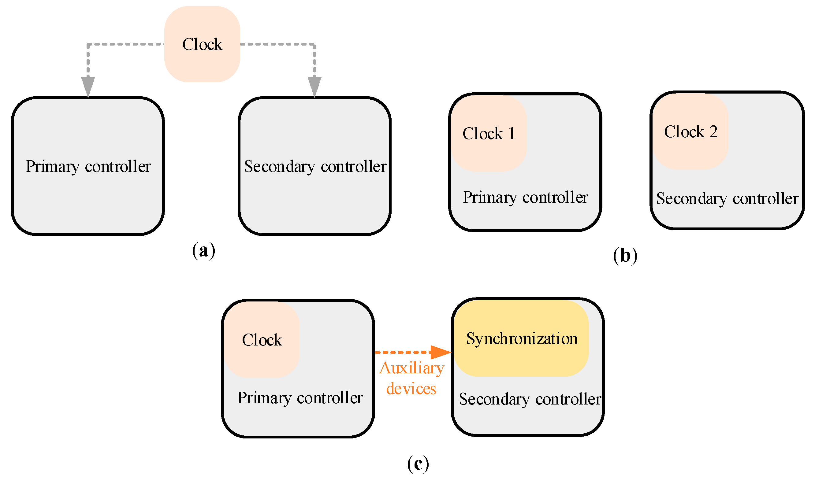
Synchronization methods of the WPT systems can be classified into three categories as elaborated in Figure 1. The first method, as shown in Figure 1a, is introducing an external clock such as general packet radio service (GPRS), code division multiple access (CDMA) and Wi-Fi. Such systems can work only in places where the communication signals are available and stable. When the signal transfer path changes, phase error will appear due to changed time delays of different controllers. Thus, this technique cannot be easily applied to systems where the transmitter and receiver spatially move with respect to each other, such as mobile phone and electric vehicle charging scenarios [25]. The second method is, installing real-time clocks on the transmitter and receiver sides as shown in Figure 1b, which can include on-board atomic clocks and precision oscillators. This method is expensive, whereas small frequency discrepancies still exist. Cumulative error occurs during a long-time operation. The third method is, considering the transmitter as a source and synchronizing the receiver using auxiliary devices as shown in Figure 1c. The feasibility and robustness of the third scheme is greater in these methods. In References [17,18,26,27], a sense winding on the secondary side is proposed to capture the magnetic flux generated by the primary resonant current in order for synchronization. A voltage signal on the sense winding can be induced and the phase locking loop (PLL) is used to detect the primary time sequence. However, secondary magnetic flux produces an undesired voltage, which can deteriorate the synchronization performance seriously. A compensation circuit should be added to eliminate the phase error caused by this effect, whereas the circuit parameters depend heavily on the operating conditions. As reported in Reference [17], the phase error can be about 22% when the coupling factor is decreased by 50% and 15% when the primary compensation capacitance is decreased by 20%. In Reference [20], secondary current is sampled by the sensor for synchronization. Except for the cost and frequency bandwidth of the sensors, the phase error caused by the time delay of the devices is corrected by a carefully designed and parameter-sensitive phase-shift circuit. In References [28,29], the real and reactive powers produced by the receiver are utilized to estimate the position of the voltage vector induced by the primary converter. This method requires accurate samplings of secondary high-frequency resonant current and voltage, as well as a complex processing hardware circuit and calculation algorithm. In multiple active receiver applications, the magnetic field becomes more complex, which increases the difficulty in phase compensation. Previous works largely focus on the applications and contributions of multiple active receiver WPT systems [30,31], whereas, synchronization techniques have not been explored due to their complexity.
Since time delay of the synchronization signal can lead to phase errors, it can be inferred that the accuracy of the synchronization technique is closely related to the signal transmission speed. A higher speed, therefore, corresponds to a higher accuracy. Some high speed methods typically use a laser beam for synchronization [32]. However, the authors find that the essence of synchronization is frequency locking which is independent of signal transmission speed. Generally, circuit-based methods are utilized to correct the phase errors caused by the time delay and system parameter variations [17,20]. The authors find that phase calibration can be easily achieved through software code.
This paper provides a clear illustration of the synchronization technique for the WPT systems. Four specific conditions are investigated, namely: Tuned and detuned WPT systems with one active receiver, and multiple active receiver WPT systems with and without cross coupling among receiving coils. Through summarizing the analysis of different systems, the essence of the synchronization technique is deduced and presented. Then, a universal synchronization technique belonging to the third synchronization category is elaborated and verified through experimental results. The salient contributions of this work are:
- (1)
- Presenting a detailed analysis of the synchronization technique and clearly decomposing it into independent frequency locking and reference phase calibration based on mathematical derivations;
- (2)
- Proposing an effective frequency locking circuit that has strong robustness and independence of system parameters;
- (3)
- Achieving reference phase calibration through software code without using additional phase-shift circuits, which advances in easy realization and cost effectiveness;
- (4)
- Realizing the synchronization for WPT systems with multiple active receivers.
This paper is divided into five sections. Section 2 analyzes different WPT systems with active receivers, which contributes to figuring out the essence of the synchronization technique. Based on the analysis, Section 3 presents the proposed hardware circuit and software code, aiming for frequency locking and reference phase calibration, respectively. Section 4 validates the feasibility and effectiveness of the proposed systems through experiments. Section 5 concludes this paper.
2. Synchronization Analysis
2.1. Tuned WPT System with One Active Receiver
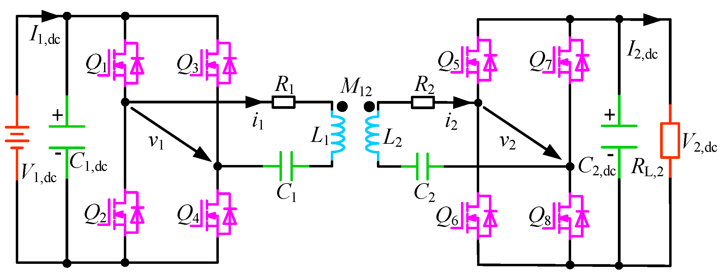
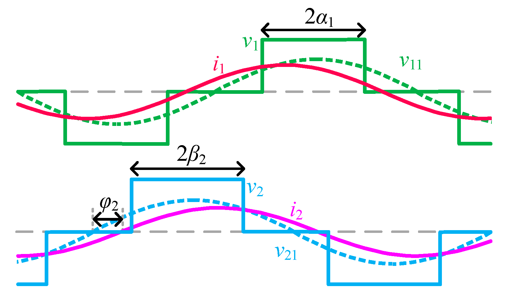
The schematic of a WPT system with one active receiver is depicted in Figure 2. V1,dc, V2,dc, I1,dc and I2,dc are the primary and secondary dc voltages and currents, respectively. C1,dc and C2,dc are the filtering capacitors and RL,2 is the load. L1 and L2 are the transmitting and receiving coils compensated by C1 and C2, respectively. R1 and R2 are the coil resistances. Q1–Q8 are eight metal-oxide-semiconductor field effect transistors (MOSFETs). v1 and v2 are the voltages applied on the resonant network, which contain only the odd frequency components. i1 and i2 are the primary and secondary resonant currents. Their fundamental frequency components are denoted as v11, v21, i11 and i21, whose root-mean-square (RMS) values are V11, V21, I11 and I21, respectively. Due to the band pass filtering effect by the resonant network, the fundamental frequency component contributes most to the transferred power. Therefore, i11 and i21 are nearly the same as i1 and i2, respectively. The typical waveforms of the system are presented in Figure 3, where v21 leads i21 by φ2. 2α1 and 2β2 represent the phase angles of the resonant voltages. In most of the previously published papers related to WPT systems, fundamental harmonic analysis (FHA) and phasor methods are widely adopted [20,21,22], which can greatly simplify the analysis. In this paper, boldface letters represent the phasors and capital italic letters represent RMS values of the phasors. For example, V11 and V11 represent the voltage phasor and RMS value of v11, respectively.
Primary and secondary parameters are identical and the inverting angular frequency ω1 is . Then, Equation (1) is obtained according to primary current loop.
Generally, the voltage across R1 is much smaller than V11. Therefore, Equation (1) can be simplified into Equation (2).
Neglecting the losses of the active bridge, energy conservation equation of the receiver can be derived as
According to fundamental harmonic analysis, V11 and V21 can be obtained.
Thus, the expression of I2,dc can be deduced as
When the primary and secondary controllers operate at different frequencies (f1 and f2, respectively), φ2 is expressed as
where φ2,0 is the initial phase of φ2. φ2,0 is determined by controllers, whereas it may be different from the coded phase.
Then, I2,dc is derived by substituting Equations (7) into (6).
When f1 = f2, I2,dc is stable. Furthermore, when φ2,0 = 0, I2,dc reaches peak value which benefits power transfer.
2.2. Detuned WPT System with One Active Receiver
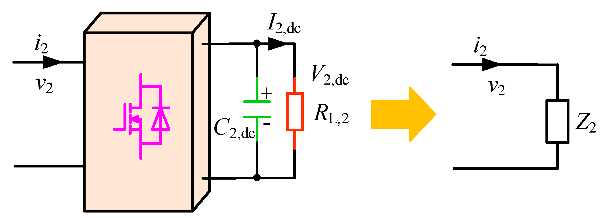
Figure 4 shows the equivalent circuit of an active bridge. Z2 represents the equivalent impedance of the active bridge on the AC side, which consists of resistive and reactive components. The phase of I21 is denoted by . Then, V21 can be expressed as
Since I2,dc = V2,dc/RL,2, Equation (3) can be deduced into Equation (10).
Therefore, I21 can be obtained and I21 can be rewritten as
The expression of Z2 can be derived as Equation (12) according to Equations (9) and (11), which is related to φ2.
Furthermore, the relationship between I2,dc and I21 can be obtained as Equation (13).
The transmitter can operate at various frequencies and the dual-side parameters can be different in practice, that is, the system can be detuned. The primary and secondary reactance are expressed as Equations (14) and (15).
Therefore, the dual-side current loops can be derived as follows.
Then, the secondary current I21 can be deduced as Equation (18).
By combining Equations (4), (13) and (18), the following equation can be obtained.
Defining the function g2(φ2) to indicate the influence of φ2 on I2,dc.
By substituting Equations (7) and (20) into Equation (19), I2,dc can be rewritten as
The output current is related to the frequency difference of the controllers and the initial phase. Without synchronization, φ2 changes periodically, resulting in the variation of g2(φ2). As a result, I2,dc will oscillate at the frequency of (f1 − f2).
2.3. Multiple Receivers without Cross Coupling
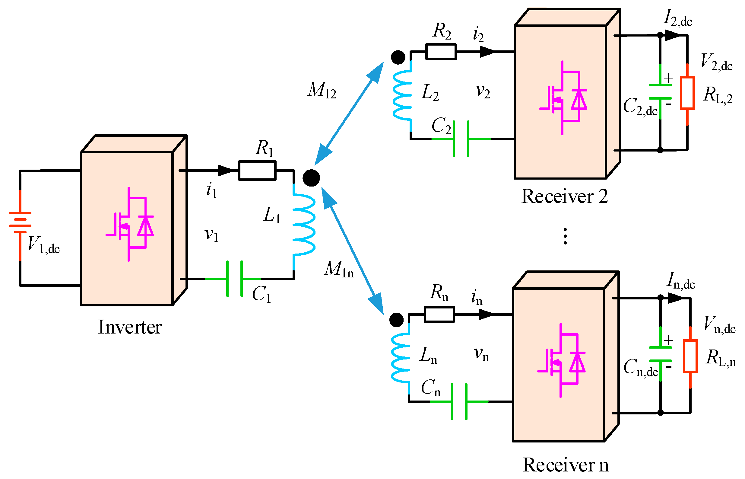
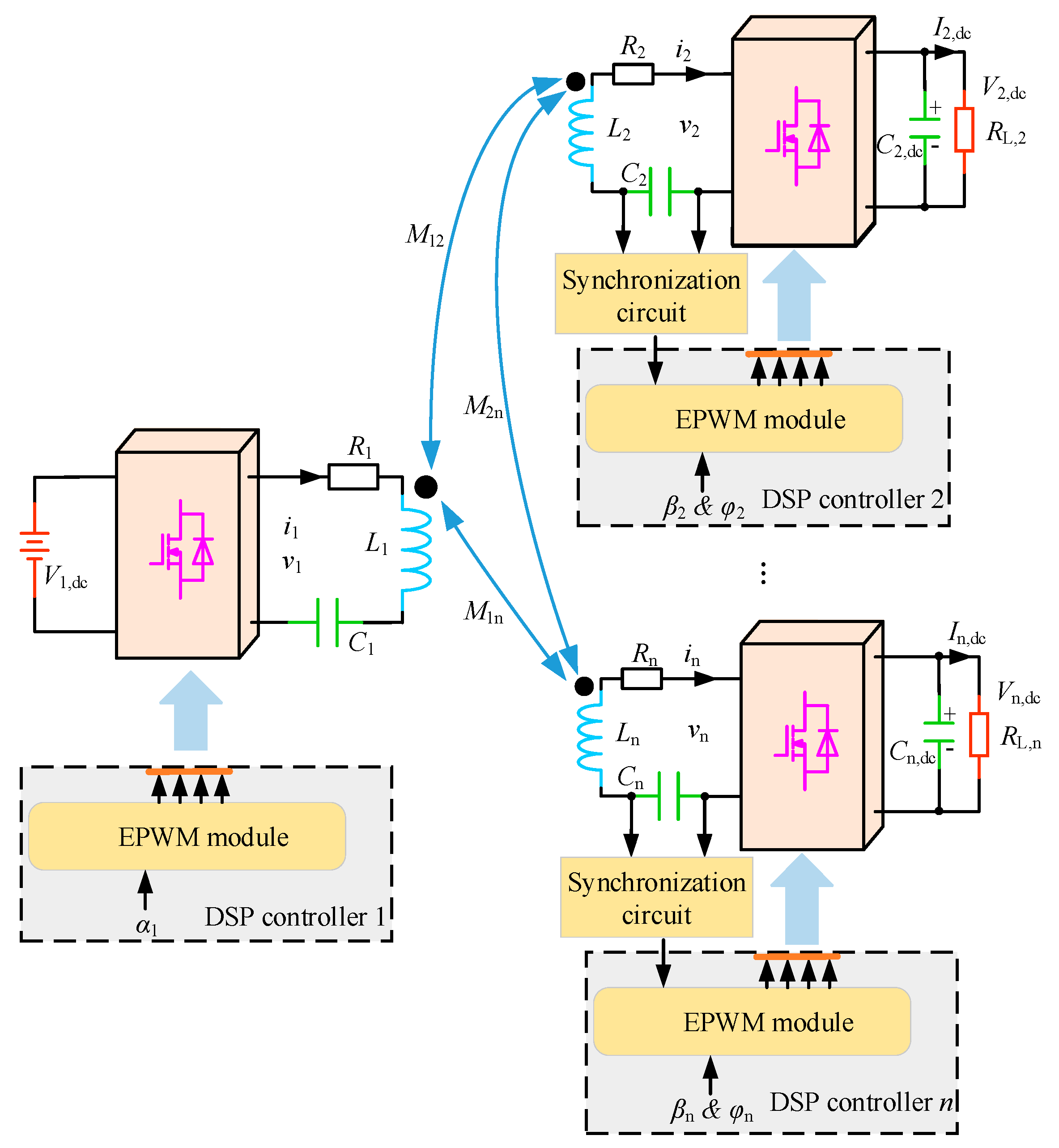
Figure 5 shows a multiple active receiver WPT system without cross coupling among the receiving coils, which has one transmitter and multiple receivers. The transmitting and receiving coils are coupled, whose mutual inductances are denoted as M1i (i ≥ 2). Li, Ri, Ci, Ci,dc and RL,i are the coil inductance, coil resistance, compensation capacitor, filtering capacitor and loading resistance of receiver i, respectively. vi, ii and Ii,dc are the resonant voltage, resonant current and output dc current, respectively.
The phase difference between vi1 and ii1 (φi) can be expressed as
where φi,0 and fi are the initial phase of φi and the operating frequency of receiver i, respectively.
Equivalent impedance Zi and reactance Xi given by Equations (23) and (24), can be obtained according to Equations (12) and (14).
The source of the system described is the primary resonant voltage. The original electromotive force of each receiver coil is induced by the primary current. Therefore, the resonant current frequencies of the receivers are supposed to be identical to the primary operating frequency. The current loops of the system are given as follows.
Primary current I11 and the receiver-side resonant current Ii1 can be deduced as Equations (27) and (28).
Thus, Ii,dc is derived based on Equation (13).
Zi is related to φi. Therefore, function gi(φ2, ..., φn) is defined to indicate the influence of φi on Ii,dc.
By substituting Equations (22) and (30) into Equation (29), Ii,dc can be rewritten as
When the cross coupling among the receiving coils is not considered, Ii,dc is a function of the operating frequency differences (f1 − fi) and the initial phases (φi,0).
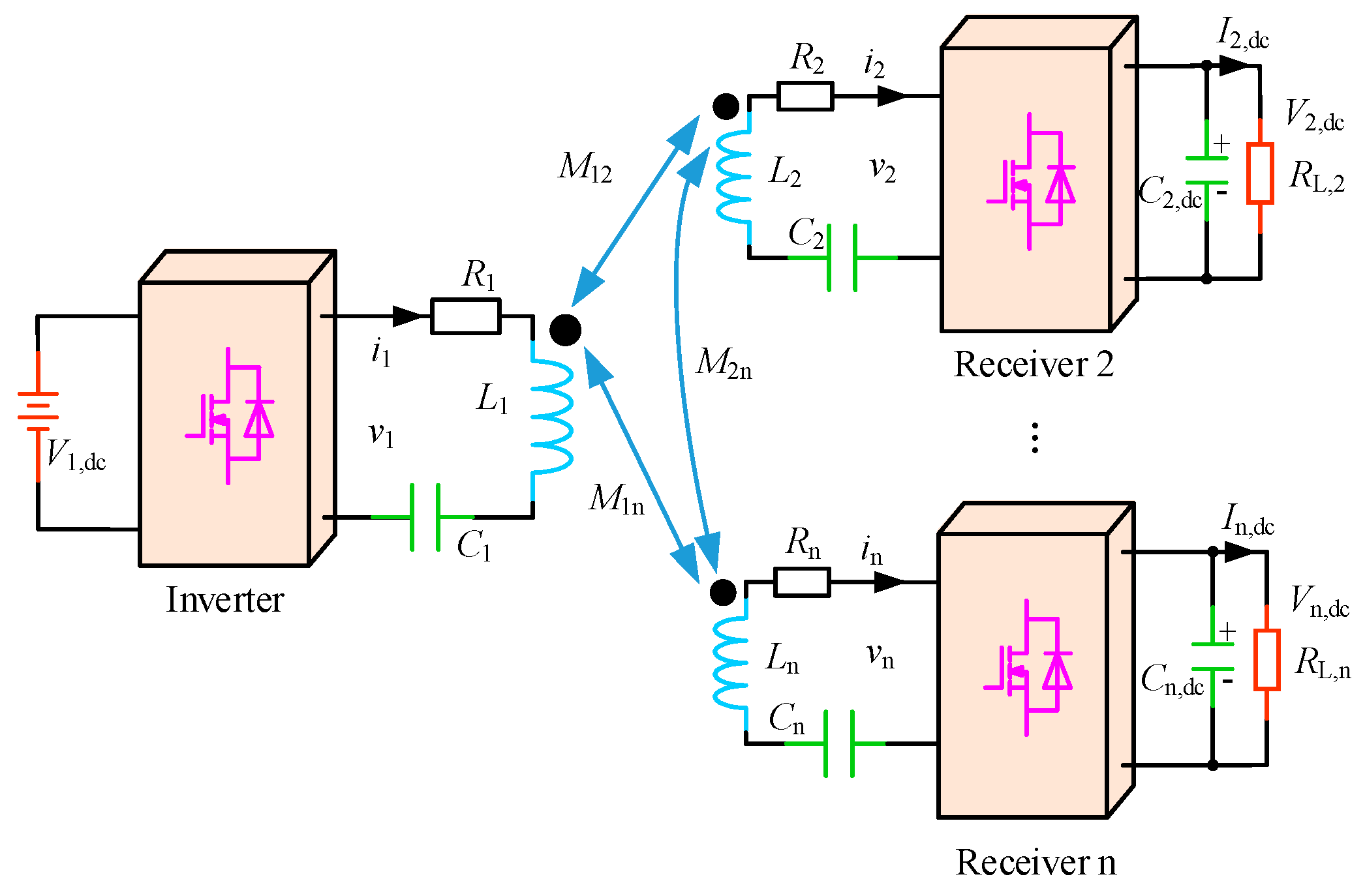
2.4. Multiple Receivers with Cross Coupling
Figure 6 shows a multiple active receiver WPT system with cross coupling among the receiving coils. The cross coupling mutual inductances are denoted as Mij (i, j ≥ 2 and i ≠ j). The current loop of receiver i can be deduced as Equation (32).
Then, the receiver-side resonant current Ii1 can be obtained by:
Thus, the expression of Ii,dc is derived.
The equivalent impedance of the receiver and the resonant currents are related to φi. Thus, function gi(φ2, ..., φn) is defined as follows.
Ii,dc can be rewritten as Equation (36).
Regardless of their tuned or detuned conditions, having one or multiple active receivers, with or without crossing coupling, the frequency of receiver-side resonant currents should be f1. It is found that Equations (8), (21), (31) and (36) can be written into a similar expression as shown in Equation (37) where ai is a constant value under a certain system configuration.
The synchronization target is to keep Ii,dc constant and find the reference phase of the receivers. Thus, the synchronization of the WPT systems can be divided into two independent functions: Ensuring that f2 = f3 = … = fn = f1 and φ2,0 = φ3,0 = … = φn,0 = 0°.
3. Proposed Synchronization Technique
The synchronization system can be decomposed into independent frequency locking and reference phase calibration as analyzed in Section 2. In this paper, the frequency locking is realized by a proposed hardware circuit and the reference phase calibration is achieved through software code.
3.1. Hardware Circuit
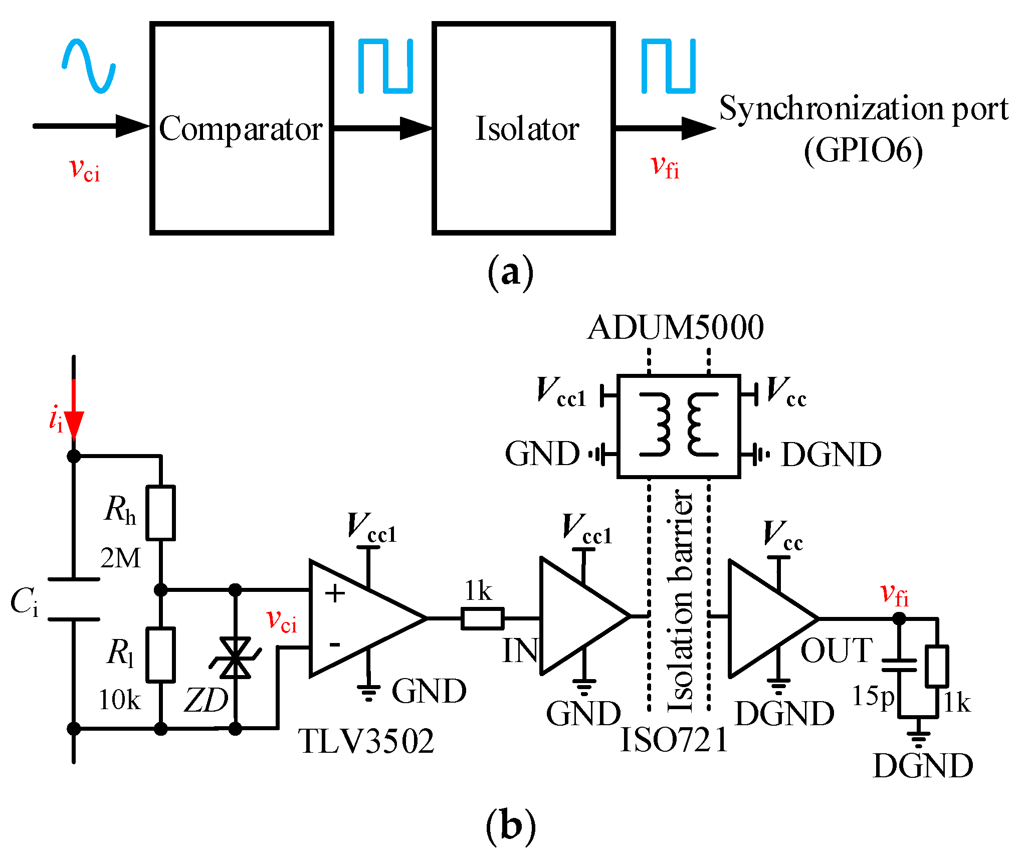
The frequency of receiver-side resonant currents should be f1. ii flows through Ci. Thus, the frequency of the voltage across Ci should be equal to f1 as well. In this paper, the voltage across the compensation capacitor is utilized for frequency locking.
Figure 7 shows the block diagram and detailed schematic of the proposed frequency locking circuit, which produces a zero-crossing synchronization signal. The voltage across Ci is divided over the resistances, which can obtain voltage vci. The high-side resistance Rh is 2 MΩ and the low-side resistance Rl is 10 kΩ. To ensure that vci stays within a proper range, the values of the divider resistances should be configured with the power level. A bidirectional Zener diode with 6.8 V reverse breakdown voltage is used to limit the voltage. vci is sent to the comparator TLV3502 (Texas Instruments, Richardson, TX, USA) which can generate a square wave with the frequency f1. After passing through the isolator ISO721 (Texas Instruments, Richardson, TX, USA), the frequency locking signal vfi is fed to the synchronization port of DSP such as GPIO6 in TMS320F28335 (Texas Instruments, Richardson, TX, USA). The comparator and the isolator are supplied by an isolated direct-current-to-direct-current (DC/DC) converter ADUM5000 (Analog Devices Inc., Wood, MA, USA). The resonant capacitor voltage is high and is converted into a digital signal immediately. Thus, the frequency locking circuit is insensitive to interferences. In addition, the circuit consists of a comparator, an isolator and an isolated power supply chip, which makes it cost effective and has a low power consumption.
3.2. Software Code
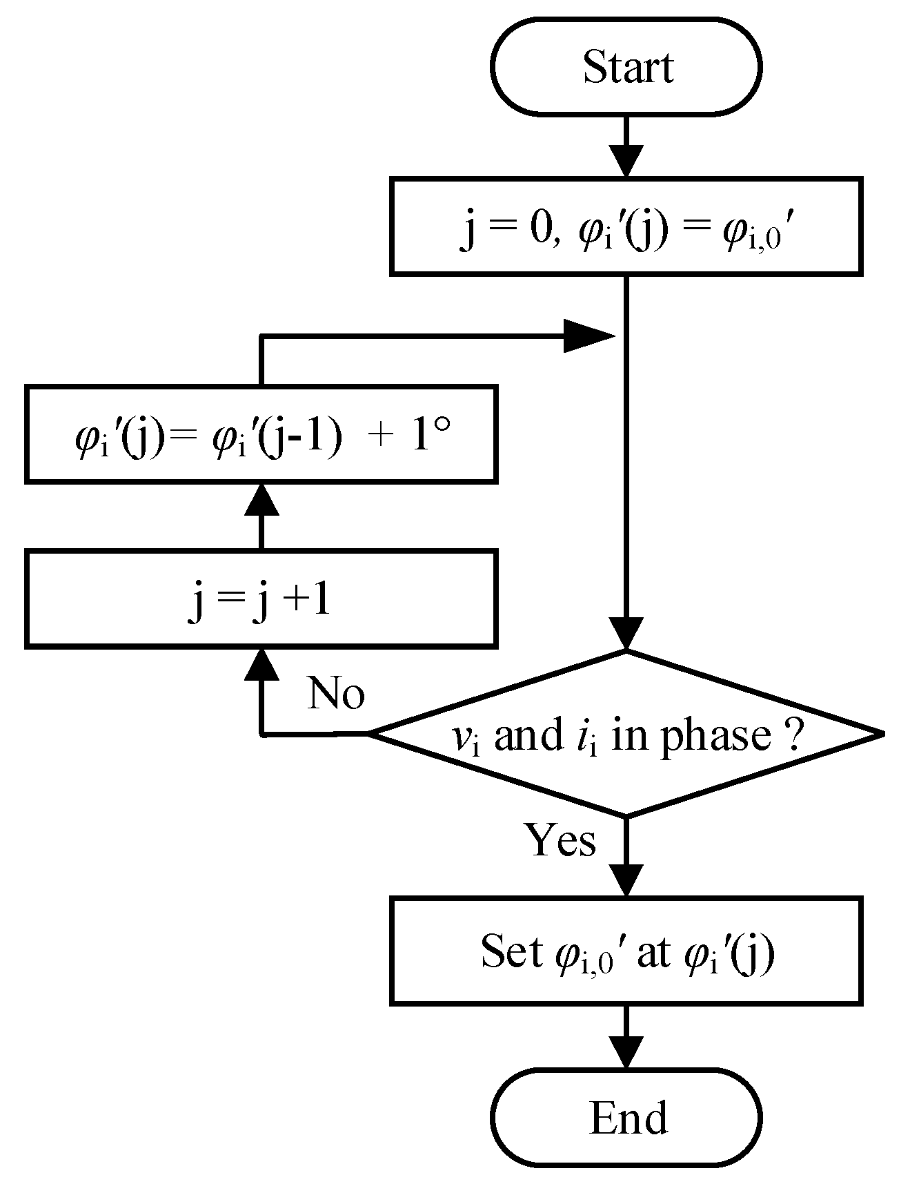
vci lags ii by 90°. However, due to the time delay of the frequency locking and the driver circuits, φi,0 in Equation (37) is uncertain and can differ from the coded initial phase. After locking the frequency, the reference phases of the controllers should be calibrated, which is implemented by software code. The coded phase defined in the controller is φi’ whose initial value is φi,0.’ The task of reference phase calibration is to change φi,0’ to ensure φi,0 = 0, that is, vi and ii are in phase. Figure 8 shows the reference phase calibration process. Firstly, φi’ is set at φi,0.’ vi and ii are captured by the oscilloscope. Then, the system is turned on and vi and ii phase synchronization is observed. If vi and ii are not in phase, traversal algorithm can be executed to change φi,’ where φi’ can vary from φi,0’ to 360° + φi,0.’ Once vi and ii are in phase, the reference phase is locked and φi,0’ is determined. Since the time delay remains almost unchanged for a certain circuit, the corresponding phase error is independent of the load, the mutual inductance and other system parameters. Furthermore, the reference phase calibration only needs one execution after the system is implemented and it can be completed within several minutes, which makes this synchronization technique easy for wide applications.
The main flowchart of the phase calibration process has been elaborated above, whereas the register configuration details are of great importance as described below. Improper configuration can lead to the system becoming unstable.
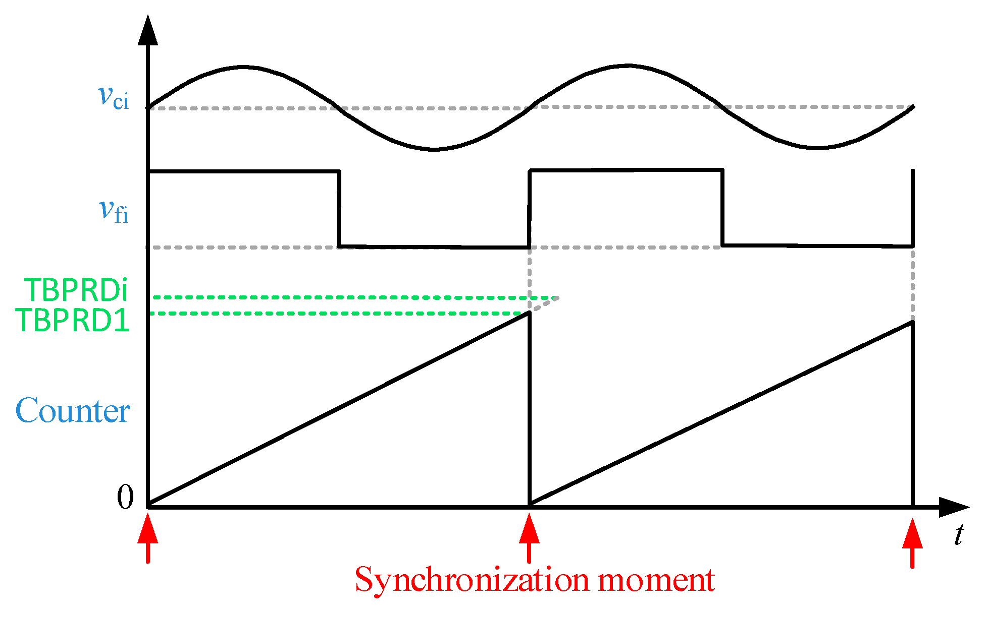
There are three counter modes of the enhanced pulse width modulator (EPWM): count-up mode, count-down mode and count-up-down mode. For easy calculation of the register values, the count-up mode is adopted in this work. The frequency locking process in the controller is shown in Figure 9, where TBPRD1 and TBPRDi (i ≥ 2) are the time base periods (TBPRD) of the PWM modules of the transmitter-side and receiver-side controllers, respectively. For better understanding, the time delay of the devices is not considered in this analysis. Ideally, time base periods can be the same. However, the actual output frequency will deviate from the preset value due to limited frequency precision. In practice, TBPRDi should be greater than TBPRD1. The receiver-side controller detects the frequency locking signal at first, where the counter should be equivalent to TBPRD1. Then, the counter is reset to 0. This process can ensure the frequency of vi equal to f1.
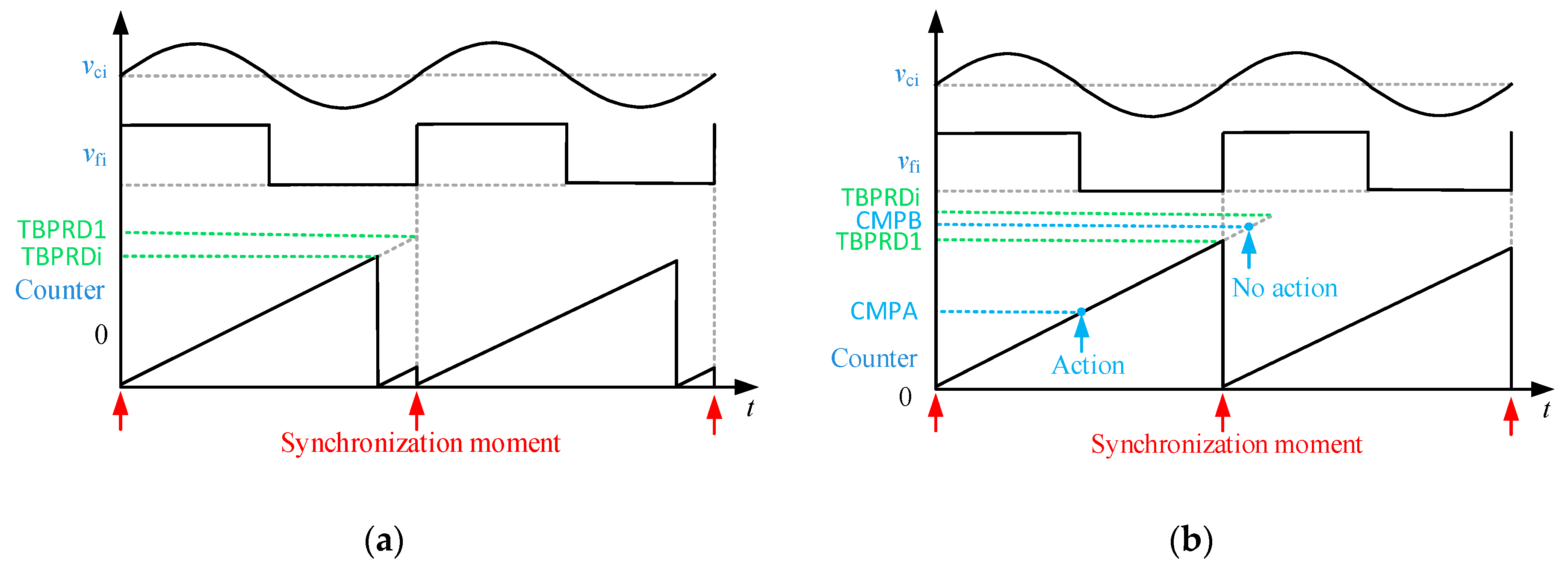
Faulty configurations of the reserved registers can lead to two problems. Firstly, as shown in Figure 10a, where TBPRDi is smaller than TBPRD1, the counter operates abnormally. The counter reaches TBPRDi and is reset to 0. When the frequency locking signal appears, the counter is reset to 0 again, resulting in a wrong counting sequence. Therefore, TBPRDi should be greater than TBPRD1. Secondly, as shown in Figure 10b, although the counter operates normally, an erroneous gate drive signal is generated. Comparing values of groups A and B (CMPA and CMPB) are used to generate βi and φi. When CMPB (or CMPA) falls into the range of (TBPRD1, TBPRDi), wrong gate drive signals appear. The counter cannot reach the reserved register value where the control signal is supposed to be toggled. Then, the gate drive signal remains unchanged, which leads to a wrong vi. Therefore, the maximum CMPA and CMPB should be slightly smaller than TBPRD1, which is denoted as CMPmax. The specific value of CMPmax should be determined according to the frequency precision of the controllers.
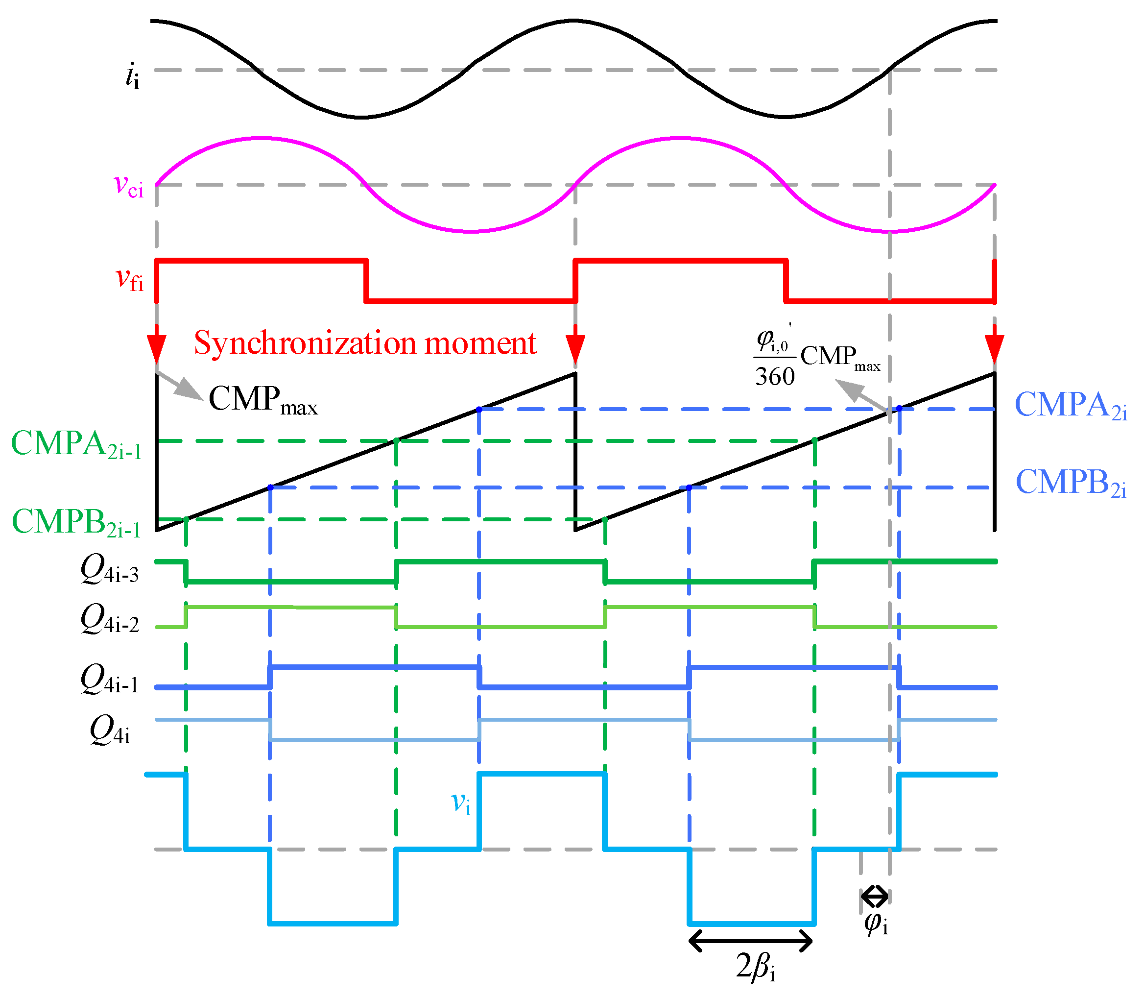
Figure 11 shows the detailed synchronization process and corresponding relationships among the reserved register values and the phase angles. The gate drive signals of receiver i are denoted as Q4i−3, Q4i−2, Q4i−1 and Q4i, whereas the comparing values of the corresponding controller are denoted as CMPA2i−1, CMPB2i−1, CMPA2i and CMPB2i. The mathematical expressions of the register values are shown in the following equations.
Since φi and φi,0’ may range from 0° to 360°, according to Equations (38)–(41), the calculated CMPA and CMPB values may be beyond [0, CMPmax]. When these values are negative or greater than CMPmax, several times of CMPmax should be added or subtracted to ensure them falling in the range.
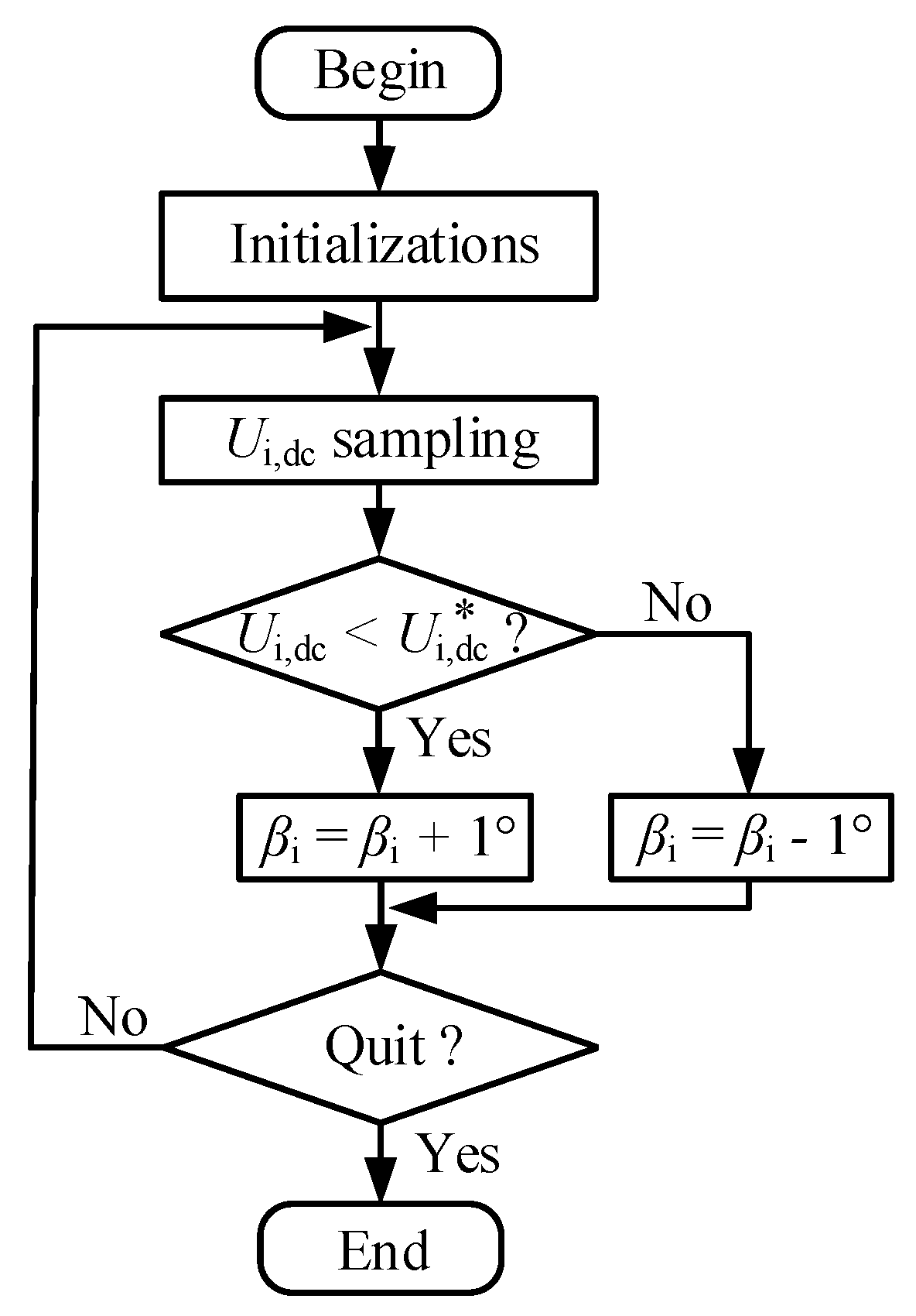
The task of reference phase calibration process is to change φi,0’ to track the point where φi = 0. After that, the receiver-side phase angles can be applied for impedance matching or output power regulation [20,21]. Many wireless charging devices require a constant voltage supply. Thus, Figure 12 shows the control flowchart for constant voltage power transfer, where Ui,dc* represents the desired voltage. If Ui,dc is greater than Ui,dc* (i.e., Ui,dc,> Ui,dc*), βi is decreased by 1°. Otherwise, βi is increased by 1°. This method is effective and easy to implement.
3.3. System Layout
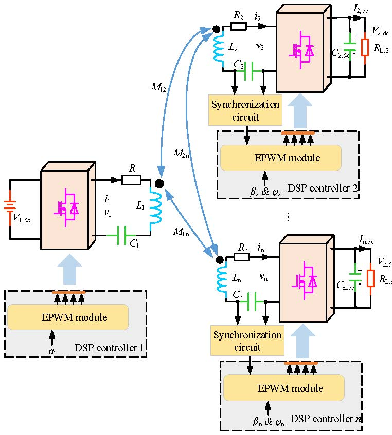
The schematic of the proposed WPT system with multiple active receivers is shown in Figure 13. A frequency locking circuit is installed on each receiver side that produces the synchronization signal for each DSP controller.
The prototype system is implemented in the following sequence: Firstly, the coded initial phase is calibrated and then the corresponding reference phase is written into the controllers. Secondly, the primary controller is turned on and the primary active bridge inverts the high frequency voltage. The frequency locking signal is generated, whereas the receiver-side controllers remain on standby and the diode rectification is used by the receivers. Thirdly, the gate drive signals of the receivers are generated. Finally, the phase angles are altered according to power transfer requirements.
4. Experiment and Discussion
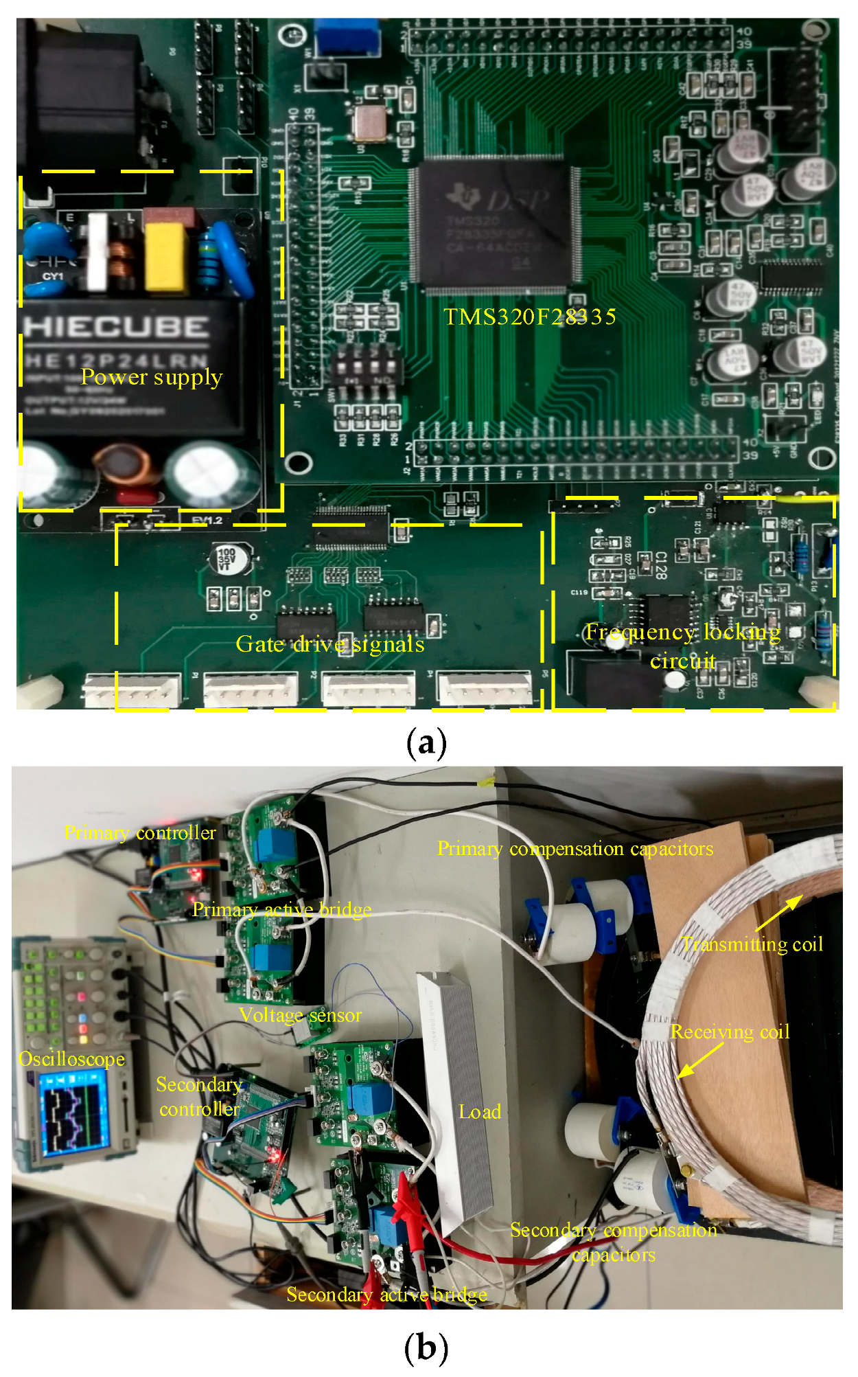
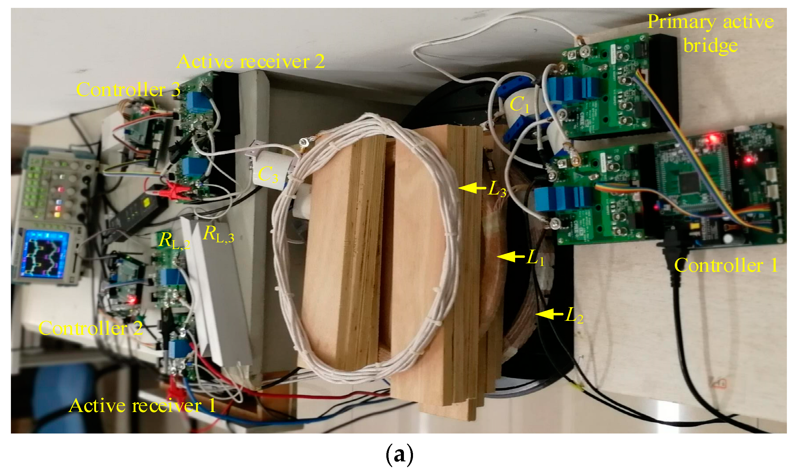
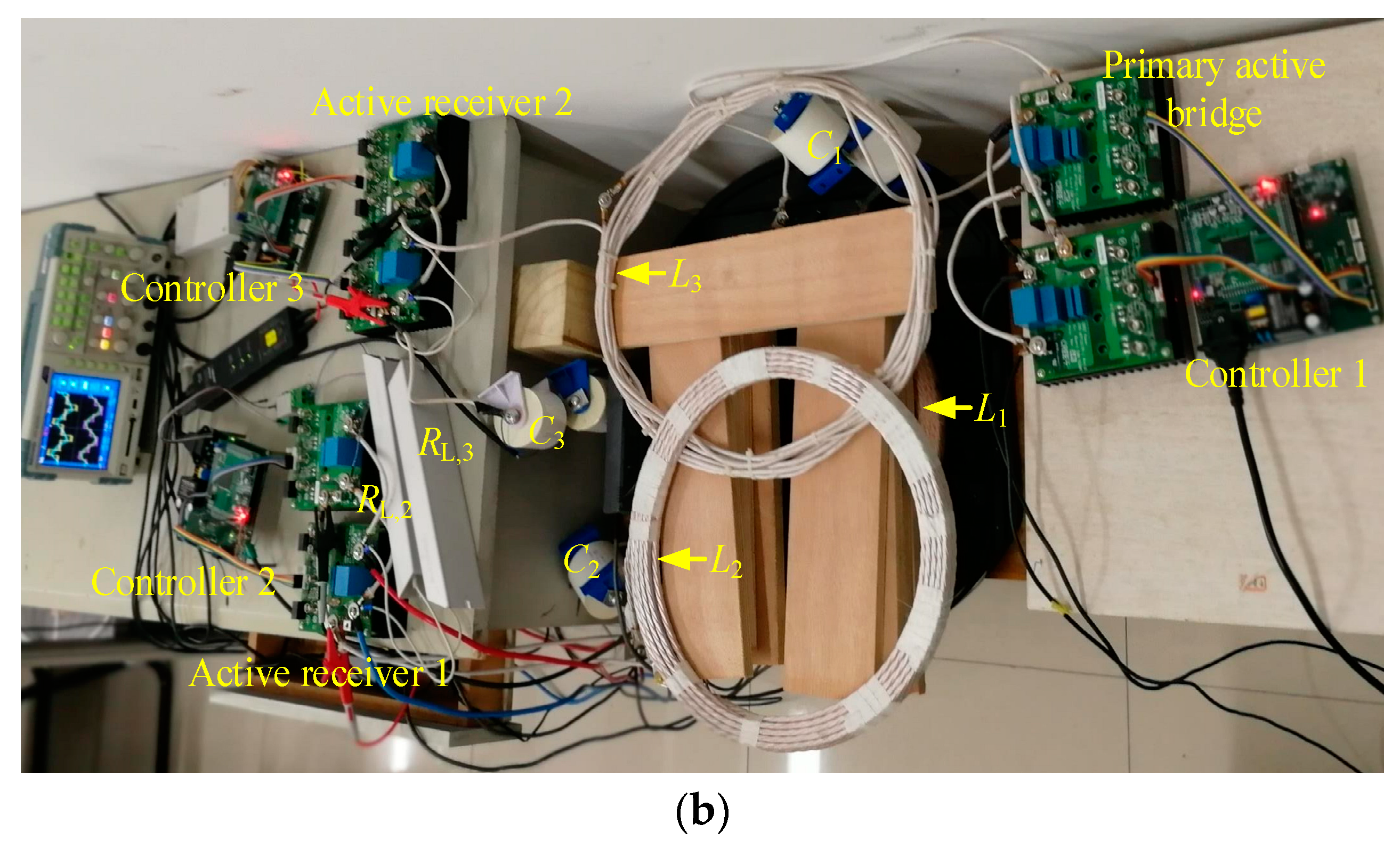
To verify the presented synchronization technique, the system is experimentally studied by using two prototypes: the first WPT system is implemented with one active receiver, whereas, the other with two active receivers. The specific parameters of the prototypes are listed in Table 1. Three independent microcontrollers and six Cree half bridges are used [33]. The coil self-inductances and mutual inductances are measured using inductance, capacitance, and resistance (LCR) meter TH2830 (RIGOL, Suzhou, China). Chroma programmable alternating-current-to-direct-current (AC/DC) electronic load model 63803 (Chroma, Marlborough, MA, USA) is utilized to vary the loading resistance. Tektronix TPS2024B Oscilloscope (Tektronix, Inc., Beaverton, OR, USA) is used to record the experimental waveforms. The experimental video is attached in Supplementary Materials.
4.1. One active Receiver WPT System
Figure 14 shows the photograph of the WPT system with one active receiver. Figure 14a shows the designed DSP controller which consists of frequency locking circuit, power supply module and DSP TMS320F28335. Figure 14b shows the view of the complete system. Both the coil inductances are 61 μH, which are compensated by 0.05 μF AC capacitors. V1,dc is 50 V. The power transfer distance (d12) is 80 mm with the mutual inductance of 16.7 μH.
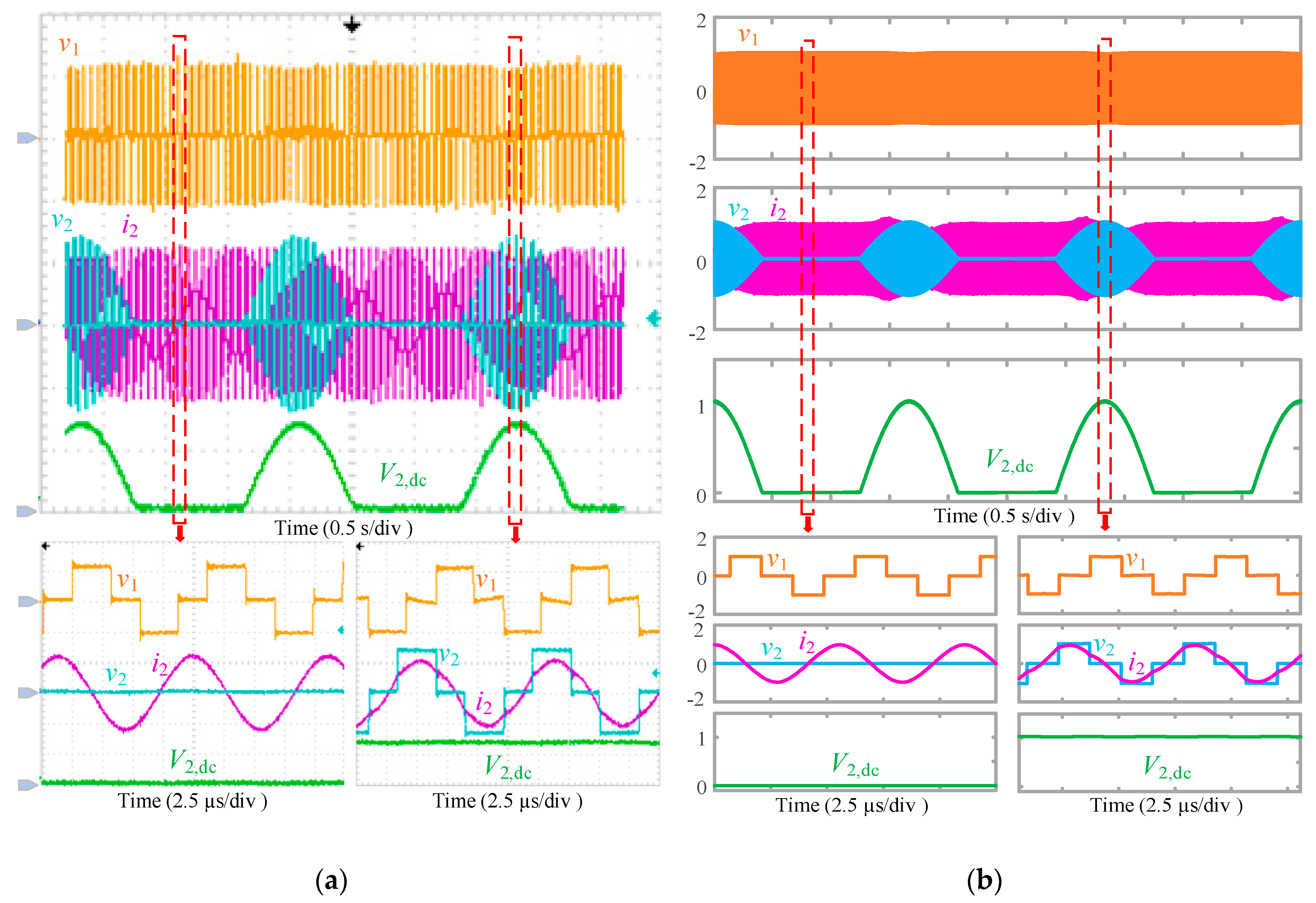
According to international standard of wireless electric vehicle charging SAE J2954 [34], the operating frequency of the WPT system ranges from 81. 38 kHz to 90 kHz. The worst possible synchronization scenario is investigated in this paper, that is, when f1 is 90 kHz. The secondary operating frequency is also set at 90 kHz. Figure 15 shows the experimental result of v1, v2, i2 and V2,dc without proposed synchronization technique. Both α1 and β2 are 45°. RL,2 is 50 Ω. The transient process is shown in the upper portion of the figure, whereas the corresponding enlarged details are shown in the lower portion. As evident from the figure, V2,dc changes periodically at a frequency about 0.6 Hz. Because of the limited frequency precision of the microcontrollers, there exists 0.6 Hz frequency difference between the transmitter and the receiver. Although the frequency difference is small compared to 90 kHz operating frequency, φ2 ranges from 0° to 360° at 0.6 Hz. Since I2,dc is a cosine function according to (8), power oscillations appear. When φ2 lies within a range of (90°, 270°), the power is transferred from the secondary side to the primary side. However, loading resistance is utilized in this experiment, which cannot provide the required power. Therefore, V2,dc becomes zero during this phase range as shown in the lower part of Figure 15a. When φ2 lies within a range of (−90°, 90°), the power is transferred to the secondary side and V2,dc is a cosine function. In simulations, the frequency of the gate drive signal is identical to the preset one, which can be used to verify the above experiment. A simulation in Simulink is implemented and f1 − f2 is set at 0.6 Hz. The simulated result in Figure 15b agrees well with the experiment, which validates the synchronization analysis. It can be concluded that WPT systems with active receivers cannot function normally without applying synchronization techniques.
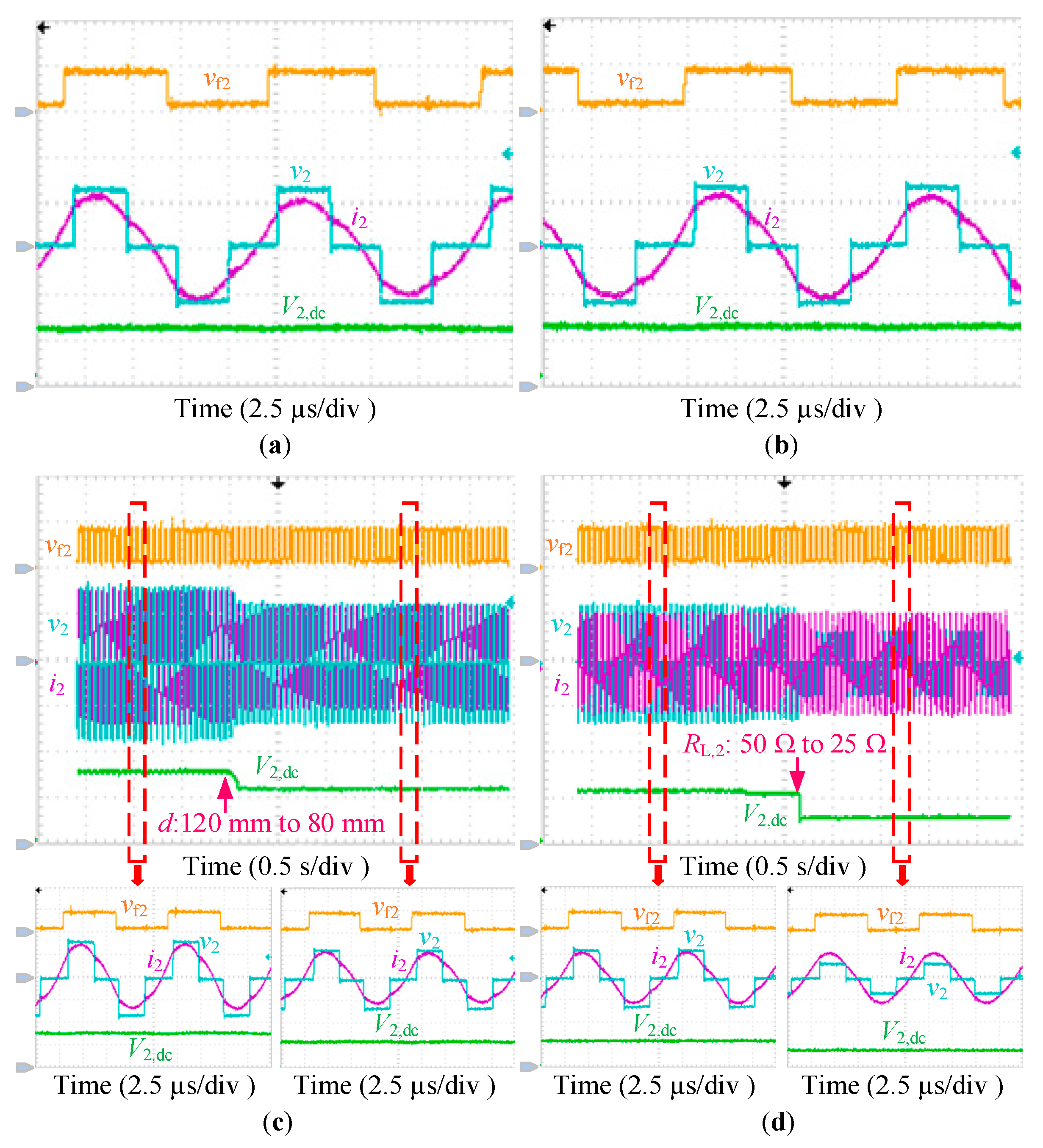
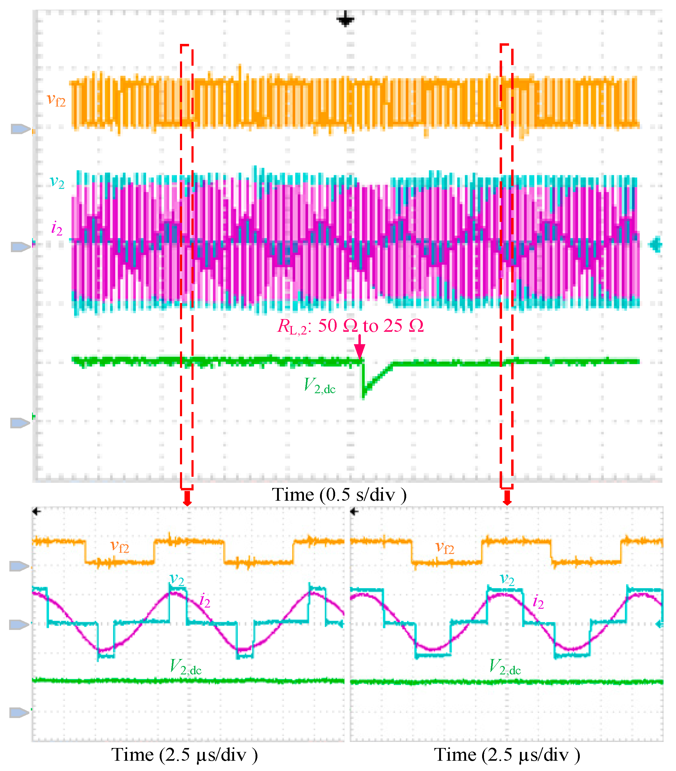
Figure 16 shows the experimental synchronization results of the proposed technique under various conditions, including vf2, v2, i2 and V2,dc. Figure 16a shows the typical experimental waveforms of the tuned WPT system. The input voltage, the phase angles and the load remain unchanged. The measured resonant frequency of the system is 91.5 kHz and the transmitter operates at this frequency. As can be seen in Figure 16a, the frequency locking signal vf2 is stable and v2 is in phase with i2. Figure 16b shows the typical waveforms of the detuned WPT system where the operating frequency is 90 kHz. The proposed synchronization technique performs well in the detuned WPT system. Figure 16c shows the experimental result during mutual inductance variation in the detuned WPT system. d12 changes from 120 mm to 80 mm, where the mutual inductance changes from 11.1 μH to 16.7 μH. V2,dc decreases with the increase of mutual inductance. As evident from the enlarged details, the system is stable and v2 is still in phase with i2. Figure 16d shows the experimental result during load variation in the detuned WPT system. RL,2 changes from 50 Ω to 25 Ω by connecting the electronic load in parallel. Although V2,dc decreases by nearly half, v2 and i2 remain in phase.
The proposed synchronization system can work effectively with variations in operating frequency, coil position and load. Then, β2 can be used to regulate the output power. Figure 17 shows the constant voltage power transfer process. The reference output voltage is set at 100 V. To guarantee the transferred power, V1,dc is increased to 80 V in this experiment. The load changes from 50 Ω to 25 Ω. To better record and observe the transition, β2 is varied by 1° each 100 millisecond in this experiment. As evident from the figures, β2 increases with decreasing RL,2 to supply more power and V2,dc stabilizes at the desired 100 V within 0.25 s. The setting period can be decreased by reducing the observation time and increasing the increment or decrement to β2. The received power increases from 200 W to 400 W and the dc-to-dc efficiency increases from 91.5% to 92.3%. For operational convenience, a magnetic core has not been used on the receiver side. The coupling factor can be increased by installing a magnetic core, which can improve the overall efficiency.
4.2. Multiple Active Receiver Wpt System
Figure 18a,b show the photographs of the multiple active receiver WPT systems without and with cross coupling between receiver-side coils, respectively. V1,dc is 50 V and α1 is set at 45°. RL,2 and RL,3 are 50 Ω. L3 is 81 μH, compensated by 0.04 μF AC capacitor. The calculated resonant frequency of receiver 2 is 88.5 kHz. The systems operates at 90 kHz, that is, the complex detuned condition. To confirm that the receivers can work under different conditions, β2 is set at 45° and β3 at 30°. In Figure 18a, the transmitting coil lies in the middle and the cross coupling between the two receiving coils is neglected. Both d12 and d13 are 80 mm. M12 and M13 are 21.2 μH and 16.7 μH, respectively. In Figure 18b, the receivers are put on the above. Except for the mutual inductances among the coils, the system parameters remain the same. M12, M13 and M23 are 8.9 μH, 11.7 μH and 4.8 μH, respectively. The cross coupling mutual inductance between the receiving coils is comparable with the mutual inductances.
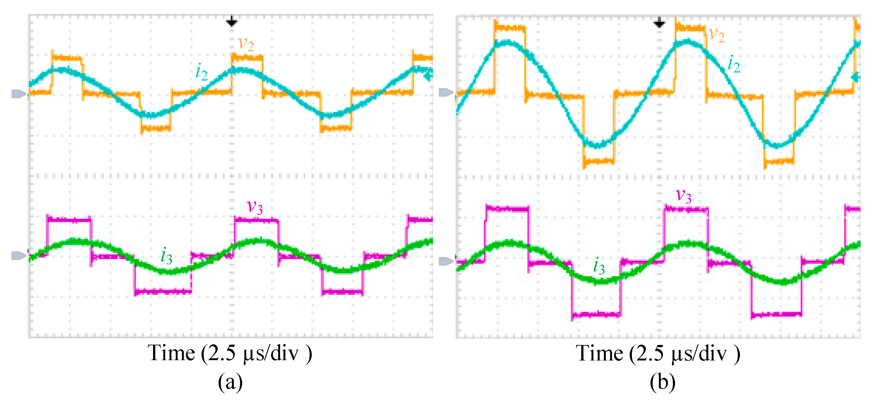
Figure 19a shows the typical waveforms of the successful synchronization result without crossing coupling, including v2, i2, v3 and i3. As evident from the figure, v2 and v3 are in phase with i2 and i3, respectively. The power is transferred to the active receivers successfully. Figure 19b shows the typical waveforms of the system with cross coupling between two receiver-side coils. The synchronization system performs well and the WPT system is stable. These experiments confirm the feasibility of the proposed synchronization technique in multiple active receiver WPT systems.
4.3. Discussion
This paper provides a comprehensive synchronization analysis of different WPT systems and decomposes the synchronization system into independent frequency locking and reference phase calibration. Table 2 summarizes the comparisons of different synchronization techniques. The inverter’s operating frequency is 20 kHz in References [6,17], 30 kHz in Reference [20] and 85 kHz in Reference [29]. A higher operating frequency can amplify the phase errors observed in Reference [17]. Thus, the synchronization difficulty increases with the increasing frequency. The proposed system can operate at 90 kHz, validating the effectiveness of proposed frequency locking method. In addition, the proposed synchronization technique is independent of system parameters and the phase error can be calibrated in advance. Thus, it can perform well under different conditions such as frequency variation, mutual inductance variation, load variation and so forth. Usually, a critical and parameter-sensitive phase-shift circuit is needed to compensate the phase error caused by time delay. However, it is easier to achieve reference phase calibration by software code, which reduces the complexity and cost of the synchronization circuit. Although the proposed technique is validated through a resistance load, it can be effectively applied to battery charging and bidirectional power transfer systems.
5. Conclusions
This paper presents a detailed synchronization analysis of WPT systems with active receivers. The synchronization problem is decomposed into two independent parts: frequency locking and reference phase calibration. Based on the analysis, a novel synchronization technique is proposed where frequency locking is realized through the hardware circuit and reference phase calibration is achieved through software code, which is a great progress for synchronization system design. In experiments, frequency locking can be realized at 90 kHz and reference phase calibration only requires one execution after the system is implemented. The proposed synchronization technique adapts to multiple active receivers under tuned and detuned conditions. In addition, the synchronization system performs well when key system parameters vary. Constant voltage power transfer can be realized with 92.3% dc-to-dc efficiency at 400 W received power. The feasibility and effectiveness of the proposed synchronization technique have been verified by theoretical analysis and experimental results.
Supplementary Materials
The following are available online at https://zenodo.org/record/1485267#.W-qdtFLFKJ0.
Author Contributions
X.L., H.T. and X.Y. conceptualized the main idea of this research project; X.L. designed and conducted the experiments with the help of T.W.; N.J. and X.Y. checked the results. X.L. wrote the whole paper; N.J. and K.H. reviewed and edited the paper.
Funding
This research was funded by United Foundation of NSFC-Henan, grant number U1604136. The APC was funded by Xijun Yang.
Conflicts of Interest
The authors declare no conflict of interest.
References
- Kurs, A.; Karalis, A.; Moffatt, R.; Joannopoulos, J.D.; Fisher, P.; Soljacic, M. Wireless power transfer via strongly coupled magnetic resonances. Science 2007, 317, 83–86. [Google Scholar] [CrossRef] [PubMed]
- Almohaimeed, A.M.; Amaya, R.E.; Lima, J.A.; Yagoub, M.C.E. An Adaptive Power Harvester with Active Load Modulation for Highly Efficient Short/Long Range RF WPT Applications. Electronics 2018, 7, 125. [Google Scholar] [CrossRef]
- He, X.; Shu, W.; Yu, B.; Ma, X. Wireless Power Transfer System for Rotary Parts Telemetry of Gas Turbine Engine. Electronics 2018, 7, 58. [Google Scholar] [CrossRef]
- Wang, T.; Liu, X.; Jin, N.; Tang, H.; Yang, X.; Ali, M. Wireless Power Transfer for Battery Powering System. Electronics 2018, 7, 178. [Google Scholar] [CrossRef]
- Liu, X.; Wang, T.; Jin, N.; Habib, S.; Ali, M.; Yang, X.; Tang, H. Analysis and Elimination of Dead-Time Effect in Wireless Power Transfer System. Energies 2018, 11, 1577. [Google Scholar] [CrossRef]
- Li, Y.; Mai, R.; Liu, Y.; He, Z. Efficiency optimising strategy for dual coupled transmitters based WPT systems. Electron. Lett. 2016, 52, 1877–1879. [Google Scholar] [CrossRef]
- Colak, K.; Asa, E.; Bojarski, M.; Czarkowski, D.; Onar, O.C. A Novel Phase-Shift Control of Semibridgeless Active Rectifier for Wireless Power Transfer. IEEE Trans. Power Electron. 2015, 30, 6288–6297. [Google Scholar] [CrossRef]
- Tan, L.; Guo, J.; Huang, X.; Liu, H.; Wang, W.; Yan, C.; Zhang, M.; Yan, C.; Zhang, M. Coordinated source control for output power stabilization and efficiency optimization in WPT systems. IEEE Trans. Power Electron. 2018, 33, 3613–3621. [Google Scholar] [CrossRef]
- Fu, M.; Yin, H.; Zhu, X.; Ma, C. Analysis and tracking of optimal load in wireless power transfer systems. IEEE Trans. Power Electron. 2015, 30, 3952–3963. [Google Scholar] [CrossRef]
- Nauryzbayev, G.; Rabie, K.M.; Abdallah, M.; Adebisi, B. On the Performance Analysis of WPT-based Dual-Hop AF Relaying Networks in α-μ Fading. IEEE Access 2018, 6, 37138–37149. [Google Scholar] [CrossRef]
- Huang, Y.; Shinohara, N.; Mitani, T. A Constant Efficiency of Rectifying Circuit in an Extremely Wide Load Range. IEEE Trans. Microw. Theory Tech. 2018, 62, 986–993. [Google Scholar] [CrossRef]
- Fu, M.; Zhang, T.; Zhu, X.; Ma, C. A 13.56 MHz wireless power transfer system without impedance matching networks. In Proceedings of the 2013 IEEE Wireless Power Transfer Conference (WPTC), Perugia, Italy, 15–16 May 2013; pp. 222–225. [Google Scholar]
- Lee, J.; Han, B. A bidirectional wireless power transfer EV charger using self-resonant PWM. IEEE Trans. Power Electron. 2015, 30, 1784–1787. [Google Scholar] [CrossRef]
- Liu, X.; Wang, T.; Yang, X.; Jin, N.; Tang, H. Analysis and Design of a Wireless Power Transfer System with Dual Active Bridges. Energies 2017, 10, 1588. [Google Scholar] [CrossRef]
- Berger, A.; Agostinelli, M.; Vesti, S.; Oliver, J.A.; Cobos, J.A.; Huemer, M. A Wireless Charging System Applying Phase-Shift and Amplitude Control to Maximize Efficiency and Extractable Power. IEEE Trans. Power Electron. 2015, 30, 6338–6348. [Google Scholar] [CrossRef]
- Neath, M.J.; Swain, A.K.; Madawala, U.K.; Thrimawithana, D.J. An optimal PID controller for a bidirectional inductive power transfer system using multiobjective genetic algorithm. IEEE Trans. Power Electron. 2014, 29, 1523–1531. [Google Scholar] [CrossRef]
- Thrimawithana, D.J.; Madawala, U.K.; Neath, M. A Synchronization Technique for Bidirectional IPT Systems. IEEE Trans. Ind. Electron. 2013, 60, 301–309. [Google Scholar] [CrossRef]
- Madawala, U.K.; Thrimawithana, D.J. A bi-directional inductive power interface for electric vehicles in V2G systems. IEEE Trans. Ind. Electron. 2011, 58, 4789–4796. [Google Scholar] [CrossRef]
- Mohamed, A.A.S.; Berzoy, A.; Mohammed, O. Experimental validation of comprehensive steady-state analytical model of bidirectional WPT system in EVs applications. IEEE Trans. Veh. Technol. 2017, 66, 5584–5594. [Google Scholar] [CrossRef]
- Mai, R.; Liu, Y.; Li, Y.; Yue, P.; Cao, G.; He, Z. An Active Rectifier Based Maximum Efficiency Tracking Method Using an Additional Measurement Coil for Wireless Power Transfer. IEEE Trans. Power Electron. 2018, 33, 716–728. [Google Scholar] [CrossRef]
- Liu, X.; Wang, T.; Yang, X.; Tang, H. Analysis of Efficiency Improvement in Wireless Power Transfer System. IET Power Electron. 2018, 11, 302–309. [Google Scholar] [CrossRef]
- Diekhans, T.; De Doncker, R.W. A dual-side controlled inductive power transfer system optimized for large coupling factor variations and partial load. IEEE Trans. Power Electron. 2015, 30, 6320–6328. [Google Scholar] [CrossRef]
- Bac, X.N.; Vilathgamuwa, D.M.; Foo, G.H.B.; Wang, P.; Ong, A.; Madawala, U.K.; Trong, D.N. An Efficiency Optimization Scheme for Bidirectional Inductive Power Transfer Systems. IEEE Trans. Power Electron. 2015, 30, 6310–6319. [Google Scholar]
- TI Inc. TMS320x2833x, 2823x High Resolution Pulse Width Modulator (HRPWM) Reference Guide; TI Inc.: Dallas, TX, USA, 2009. [Google Scholar]
- Zhao, L.; Thrimawithana, D.J.; Madawala, U.K. Hybrid Bidirectional Wireless EV Charging System Tolerant to Pad Misalignment. IEEE Trans. Ind. Electron. 2017, 64, 7079–7086. [Google Scholar] [CrossRef]
- Thrimawithana, D.J.; Madawala, U.K.; Neath, M.; Geyer, T. A sense winding based synchronization technique for bidirectional IPT pick-ups. In Proceedings of the 2011 IEEE Energy Conversion Congress and Exposition (ECCE), Phoenix, AZ, USA, 17–22 September 2011; pp. 1405–1410. [Google Scholar]
- Son, Y.; Ha, J.I. Data transmission method without additional circuits in bidirectional wireless power transfer system. In Proceedings of the Applied Power Electronics Conference and Exposition (APEC), Long Beach, CA, USA, 20–24 March 2016; pp. 3717–3721. [Google Scholar]
- Thrimawithana, D.J.; Madawala, U.K.; Neath, M. A P&Q based synchronization technique for Bi-directional IPT pick-ups. In Proceedings of the 2011 IEEE Ninth International Conference on Power Electronics and Drive Systems (PEDS), Singapore, 5–8 December 2011; pp. 40–45. [Google Scholar]
- Tang, Y.; Chen, Y.; Madawala, U.K.; Thrimawithana, D.J.; Ma, H. A New Controller for Bi-directional Wireless Power Transfer Systems. IEEE Trans. Power Electron. 2018, 33, 9067–9087. [Google Scholar] [CrossRef]
- Mai, R.; Ma, L.; Liu, Y.; Yue, P.; Cao, G.; He, Z. A Maximum Efficiency Point Tracking Control Scheme Based on Different Cross Coupling of Dual-Receiver Inductive Power Transfer System. Energies 2017, 10, 217. [Google Scholar] [CrossRef]
- Swain, A.K.; Devarakonda, S.; Madawala, U.K. Modeling, sensitivity analysis, and controller synthesis of multipickup bidirectional inductive power transfer systems. IEEE Trans. Ind. Inform. 2014, 10, 1372–1380. [Google Scholar] [CrossRef]
- Zhao, R.; Gladwin, D.T.; Stone, D.A. Phase shift control based Maximum Efficiency Point Tracking in resonant wireless power system and its realization. In Proceedings of the 42nd Annual Conference of IEEE Industrial Electronics Society (IECON), Florence, Italy, 23–26 October 2016; pp. 4541–4546. [Google Scholar]
- Cree Inc. KIT8020CRD8FF1217P-1 CREE Silicon Carbide MOSFET Evaluation Kit User’s Manual; Cree Inc.: Durham, NC, USA, 2014. [Google Scholar]
- J2954™ NOV2017, SAE J2954. 2017. Available online: https://saemobilus.sae.org/content/J2954_201711 (accessed on 14 June 2018).
Figure 1.
Synchronization methods: (a) external clock; (b) precision on-board clocks; and (c) auxiliary synchronization devices.
Figure 1.
Synchronization methods: (a) external clock; (b) precision on-board clocks; and (c) auxiliary synchronization devices.

Figure 2.
WPT system with one active receiver.

Figure 3.
Typical primary and secondary waveforms of a WPT system with one active receiver.

Figure 4.
Equivalent circuit of active bridge.

Figure 5.
Schematic of a multiple active receiver WPT system without cross coupling.

Figure 6.
Schematic of a multiple active receiver WPT system with cross coupling.

Figure 7.
Proposed frequency locking circuit: (a) block diagram; and (b) detailed schematic.

Figure 8.
Reference phase calibration process.

Figure 9.
Synchronization process.

Figure 10.
Faulty configuration of reserved registers: (a) wrong counting sequence; and (b) comparing value beyond the counting range.
Figure 10.
Faulty configuration of reserved registers: (a) wrong counting sequence; and (b) comparing value beyond the counting range.

Figure 11.
Detailed synchronization process and corresponding relationships among reserved register values and phase angles.
Figure 11.
Detailed synchronization process and corresponding relationships among reserved register values and phase angles.

Figure 12.
Flowchart of constant voltage power transfer.

Figure 13.
System schematic.

Figure 14.
Photograph of WPT system with one active receiver: (a) DSP controller; and (b) overall system.
Figure 14.
Photograph of WPT system with one active receiver: (a) DSP controller; and (b) overall system.

Figure 15.
Power oscillations without synchronization: (a) experimental; and (b) simulated. v1, 50 V/div; v2 and V2,dc,100 V/div; i2, 5 A/div.
Figure 15.
Power oscillations without synchronization: (a) experimental; and (b) simulated. v1, 50 V/div; v2 and V2,dc,100 V/div; i2, 5 A/div.

Figure 16.
Experimental synchronization results of proposed technique under various conditions: (a) tuned WPT system; (b) detuned WPT system; (c) mutual inductance variation in detuned WPT system; and (d) load variation in detuned WPT system. vf2, 5 V/div; v2 and V2,dc, 100 V/div; i2, 5 A/div.
Figure 16.
Experimental synchronization results of proposed technique under various conditions: (a) tuned WPT system; (b) detuned WPT system; (c) mutual inductance variation in detuned WPT system; and (d) load variation in detuned WPT system. vf2, 5 V/div; v2 and V2,dc, 100 V/div; i2, 5 A/div.

Figure 17.
Constant voltage power transfer. vf2, 5 V/div; v2 and V2,dc, 100 V/div; i2, 10 A/div.

Figure 18.
Multiple active receiver WPT systems without and with cross coupling between receiver-side coils: (a) without cross coupling; and (b) with cross coupling.
Figure 18.
Multiple active receiver WPT systems without and with cross coupling between receiver-side coils: (a) without cross coupling; and (b) with cross coupling.


Figure 19.
Successful synchronization results of multiple active receiver systems without and with cross coupling between receiver-side coils: (a) without cross coupling; and (b) with cross coupling. v2 and v3, 50 V/div; i2 and i3, 5 A/div.
Figure 19.
Successful synchronization results of multiple active receiver systems without and with cross coupling between receiver-side coils: (a) without cross coupling; and (b) with cross coupling. v2 and v3, 50 V/div; i2 and i3, 5 A/div.


Table 1.
Key parameters of proposed system.
| Symbol | Quantity | Value |
|---|---|---|
| L1 | coil inductance of transmitter | 61 μH |
| L2 | coil inductance of receiver 1 | 61 μH |
| L3 | coil inductance of receiver 2 | 81 μH |
| C1 | primary compensation capacitance | 0.05 μF |
| C2 | compensation capacitance of receiver 1 | 0.05 μF |
| C3 | compensation capacitance of receiver 2 | 0.04 μF |
Table 2.
Comparisons of different synchronization techniques.
| Source | Operating Frequency | Frequency Variation | Mutual Induction Variation | Load Variation | Multiple Receivers | Phase Calibration Method | Complexity |
|---|---|---|---|---|---|---|---|
| [6] | 20 kHz | × | × | √ | × | N/A | N/A |
| [17] | 20 kHz | × | √ | √ | × | Circuit-based | Complex circuit and algorithm |
| [20] | 30 kHz | × | × | √ | × | Circuit-based | N/A |
| [29] | 85 kHz | × | √ | √ | × | Circuit-based | Complex circuit and algorithm |
| This paper | 90 kHz | √ | √ | √ | √ | Software Code | Simple circuit and simplified algorithm |
© 2018 by the authors. Licensee MDPI, Basel, Switzerland. This article is an open access article distributed under the terms and conditions of the Creative Commons Attribution (CC BY) license (http://creativecommons.org/licenses/by/4.0/).
Share and Cite
MDPI and ACS Style
Liu, X.; Jin, N.; Yang, X.; Wang, T.; Hashmi, K.; Tang, H. A Novel Synchronization Technique for Wireless Power Transfer Systems. Electronics 2018, 7, 319. https://doi.org/10.3390/electronics7110319
AMA Style
Liu X, Jin N, Yang X, Wang T, Hashmi K, Tang H. A Novel Synchronization Technique for Wireless Power Transfer Systems. Electronics. 2018; 7(11):319. https://doi.org/10.3390/electronics7110319
Chicago/Turabian StyleLiu, Xin, Nan Jin, Xijun Yang, Tianfeng Wang, Khurram Hashmi, and Houjun Tang. 2018. "A Novel Synchronization Technique for Wireless Power Transfer Systems" Electronics 7, no. 11: 319. https://doi.org/10.3390/electronics7110319
Note that from the first issue of 2016, this journal uses article numbers instead of page numbers. See further details here.