Fully Integrated Low-Ripple Switched-Capacitor DC–DC Converter with Parallel Low-Dropout Regulator


Microwave Embedded Circuit and System Laboratory, School of Electrical Engineering, Chung-Ang University, Seoul 06974, Korea
*
Author to whom correspondence should be addressed.
Electronics 2019, 8(1), 98; https://doi.org/10.3390/electronics8010098
Submission received: 20 November 2018
/
Revised: 5 January 2019
/
Accepted: 11 January 2019
/
Published: 16 January 2019
(This article belongs to the Special Issue Signal Processing and Analysis of Electrical Circuit)
Abstract
:In this paper, we propose a fully integrated switched-capacitor DC–DC converter with low ripple and fast transient response for portable low-power electronic devices. The proposed converter reduces the output ripple by filtering the control ripple via combining a low-dropout regulator with a main switched-capacitor DC–DC converter with a four-bit digital capacitance modulation control. In addition, the four-phase interleaved technique applied to the main converter reduces the switching ripple. The proposed converter provides an output voltage ranging from 1.2 to 1.5 V from a 3.3 V supply. Its peak efficiency reaches 73% with ripple voltages below 55 mV over the entire output power range. The transient response time for a load current variation from 100 μA to 50 mA is measured to be 800 ns. Importantly, the converter chip, which is fabricated using 0.13 μm complementary metal–oxide–semiconductor (CMOS) technology, has a size of 2.04 mm2. We believe that our approach can contribute to advancements in power sources for applications such as wearable electronics and the Internet of Things.
1. Introduction
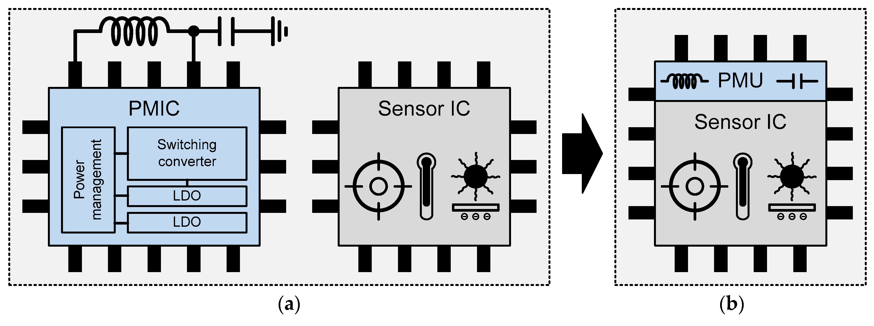
Rapid advances in the Internet of Things and wearable electronic devices have led to an increasing demand for various types of sensors [1]. For portability, such devices/applications are usually powered by small batteries, which limit the operating time of sensor-based devices. Therefore, in order to increase the battery efficiency to provide longer operating times, power management units such as power management integrated circuits (ICs) are used to control power consumption [2,3]. The power management IC can be mounted on the same printed circuit board as the sensor IC, as shown in Figure 1a. Meanwhile, certain off-chip passive components such as inductors and capacitors are additionally required for external support of the power management IC because they cannot be integrated into the chip. In this regard, although multichip configurations are convenient for a sensor module design, the cost and size of the resulting modules increase. Thus, integration of the power management unit and passive components into a single sensor chip (Figure 1b) is being actively pursued to reduce the module size and to increase market competitiveness [4,5,6,7,8,9]. The power management unit normally comprises a high-efficiency switching DC–DC converter and a linear low-dropout regulator. The switching DC–DC converter adjusts the battery voltage that drops over time to a fixed supply voltage, and its output drives the low dropout regulator to provide a voltage with low ripple and low noise to supply-sensitive analog components on the sensors [10,11].
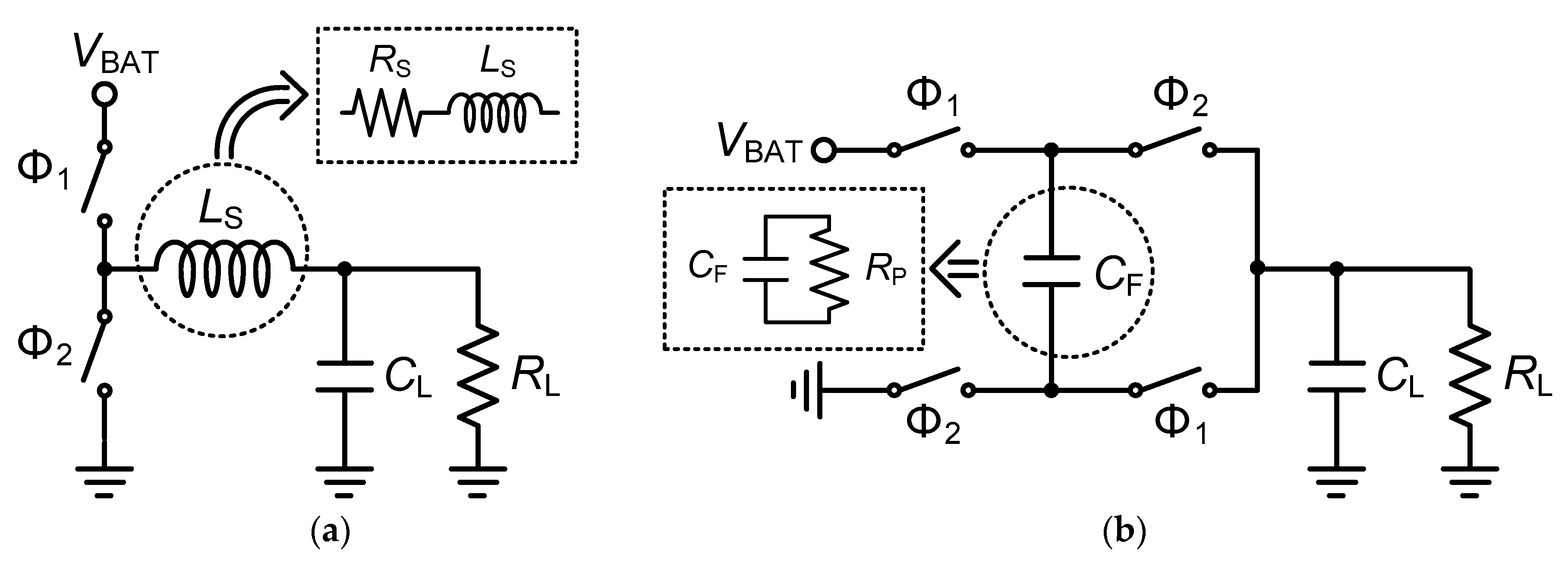
Figure 2 shows the two types of currently available switching DC–DC converters according to the choice of passive components utilized for energy storage. The first type is the inductor-based converter, which employs inductor LS and a push–pull stage as shown in Figure 2a. The output voltage is regulated by controlling the switches (Φ1 and Φ2) with either a pulse–width modulator or a pulse–frequency modulator [12,13]. The second type is the capacitor-based converter, which employs a flying capacitor CF and four switches (Φ1 and Φ2). The output voltage is regulated by controlling the switches with a pulse–width modulator, pulse–frequency modulator, or digital capacitor modulator (DCpM) [14,15,16,17]. The converting power depends on the storage capacity of the passive components as per the relation PL = L·I2/2 for the inductor-based converter and PC = C·V2/2 for the capacitor-based converter. Here, we note that inductor-based converters can deliver more power than capacitor-based converters via increasing the current at a fixed battery voltage, VBAT. Moreover, high power efficiency can be achieved by use of an off-chip inductor with high inductance and high Q values while maintaining a low ripple voltage. Thus, the traditional inductor-based buck converter has been widely adopted for moderate- to high-power applications.
On the other hand, integrated inductors based on complementary metal–oxide–semiconductor (CMOS) technology present many limitations. First, the feasible inductance LS on a chip is limited from a few to some tens of nanohenries due to the planar layout structure and fabrication cost. Thus, integrated inductor-based converters should increase the modulation frequency to maintain ripple levels; however, this also increases the switching loss. Second, series resistance RS is very high, which leads to an increased inductor loss over the switching loss, regardless of the use of expensive additional manufacturing processes involving thick metals or integrated magnetic materials. Finally, the integrated inductor exhibits power loss due to the large parasitic capacitance in relation to the substrate. In contrast, integrated capacitors afford either high parallel resistance RF or high Q factor via the metal–insulator–metal (MIM) structure. Therefore, when passive components are realized with CMOS technology, capacitors afford better energy density per chip area relative to inductors, as explained in References [18,19,20]. Consequently, capacitor-based converters exhibit better power and cost efficiency than inductor-based converters in low-power applications, such as sensors and Internet of Things devices.
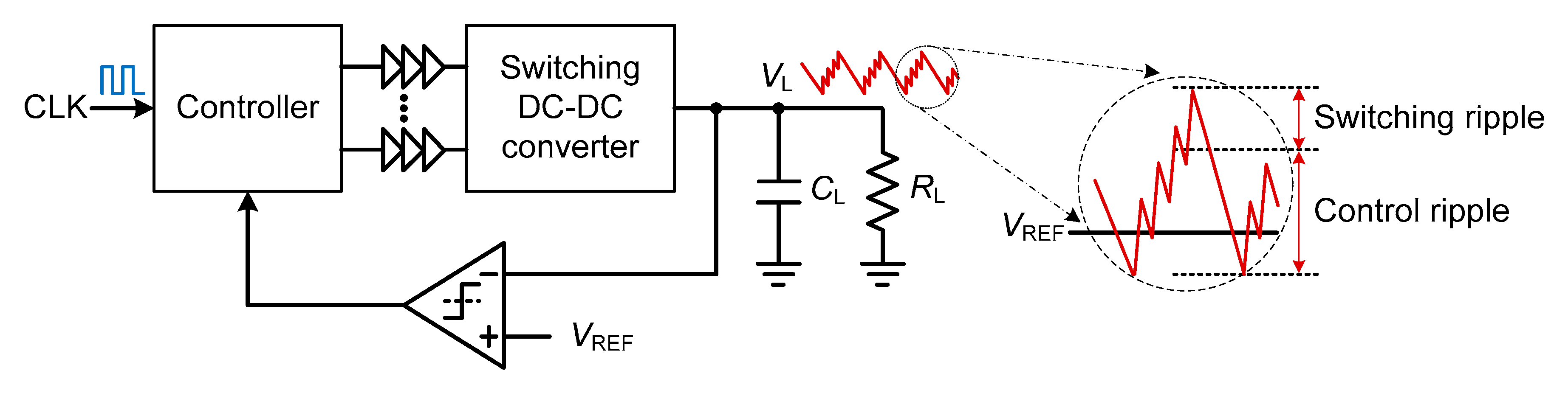
Figure 3 shows the block diagram of a commonly used switched-capacitor (SC) DC–DC converter utilizing one-boundary hysteresis feedback for output voltage regulation and its output ripple voltage. The controller provides switching control signals to the converter in phase with the input clock CLK. The one-boundary hysteresis configuration employs only one comparator for the feedback control to compare the output voltage with the reference voltage VREF [21]. In the steady state, this feedback causes a low-frequency control ripple. In addition, the SC DC–DC converter “dumps” the charge from the input to the flying capacitor and from the capacitor to the output at discrete time intervals according to the clock frequency. This discrete charge transfer causes an unavoidable switching ripple. The switching ripple is usually lower than the control ripple because the switching frequency is higher than the control frequency.
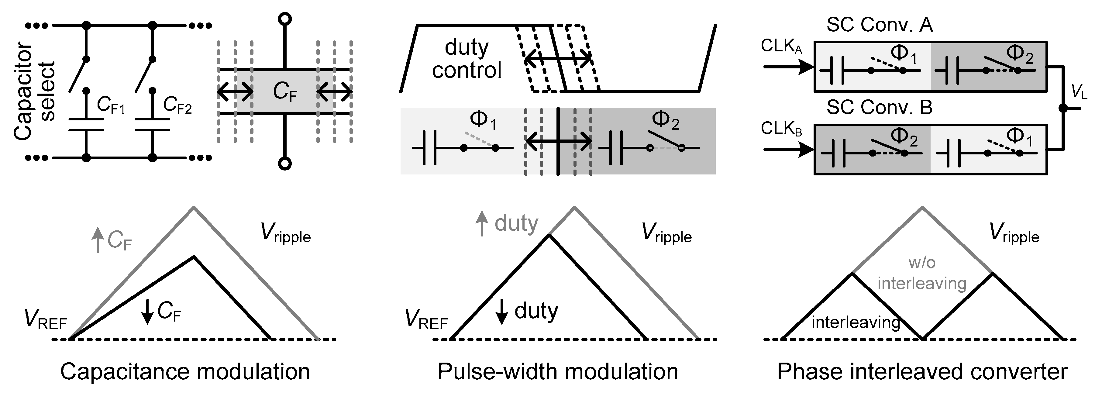
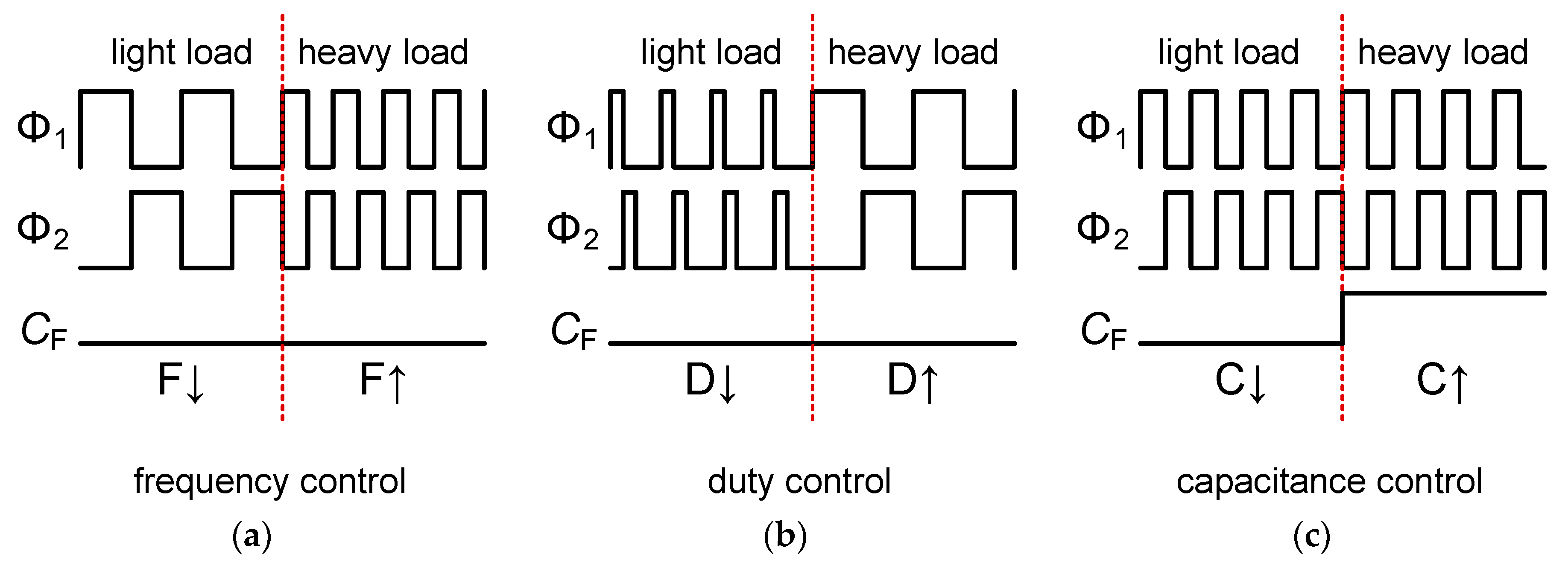
Fully integrated SC DC–DC converters require additional techniques to suppress the ripple due to the size limitations of the load and flying capacitors. Figure 4 shows three representative ripple mitigation techniques applied to the SC DC–DC converters. The capacitance modulation technique regulates the capacity of the flying capacitor, which transfers the charge to the load, to suppress the ripple. Flying capacitors are divided into several capacitors controlled by digital codes [15]. The capacitance modulation operates as a low-capacity flying capacitor in the light-load state and is controlled to operate as a high-capacity flying capacitor in the heavy-load state. Further, pulse–width modulation controls the time for which the flying capacitor is connected to the load. This method reduces the ripple by regulating the amount of charge delivered to the load per clock cycle [22].
The multiphase interleaving technique divides a converter into multiple units and drives each unit in a different clock phase [19]. Because each converter operates in different phases, it appears that the ripple waveform is operating at a frequency that is equal to the number of interleaved phases. The ripple is reduced by the number of interleaved phases.
Against this backdrop, here, we propose a low-ripple fast-transient SC DC–DC converter operating over the output current range, which integrates all the active and passive components on a single chip. The converter employs a two-boundary hysteresis control with interleaving through a four-bit DCpM to reduce the switching ripple and a parallel low-dropout regulator (LDR) to considerably mitigate the ripple.
2. Principles of SC DC–DC Converters
2.1. Operation of the 2:1 Step-Down SC DC–DC Converter
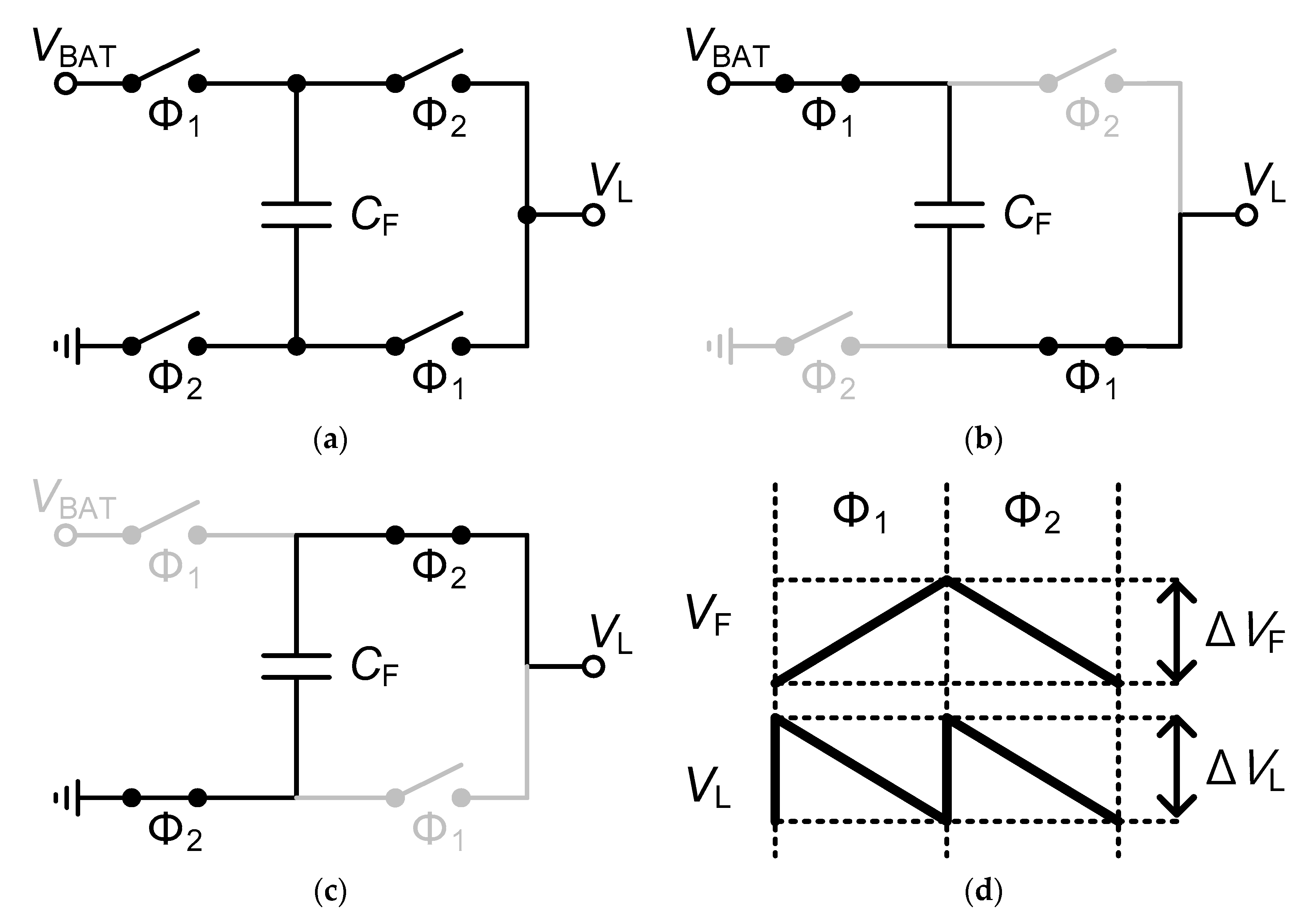
The 2:1 step-down SC DC–DC converter operates in the two phases, as shown in Figure 5. The output voltage is half the input voltage under ideal operation. Hence, maximum efficiency can only be achieved if each phase operates at 50% duty cycle. During phase 1 (Φ1), the flying capacitor is connected between the input node VBAT and output node VL, as shown in Figure 5b. In this phase, the flying capacitor is charged up to the voltage difference between VBAT and VL. During phase 2 (Φ2), the flying capacitor is connected to VL and the ground, as shown in Figure 5c. The charge acquired by the flying capacitor during phase 1 is supplied to the output node. The repeated charging and discharging during these phases produce output voltage ripple ΔVL, as illustrated in Figure 5d.
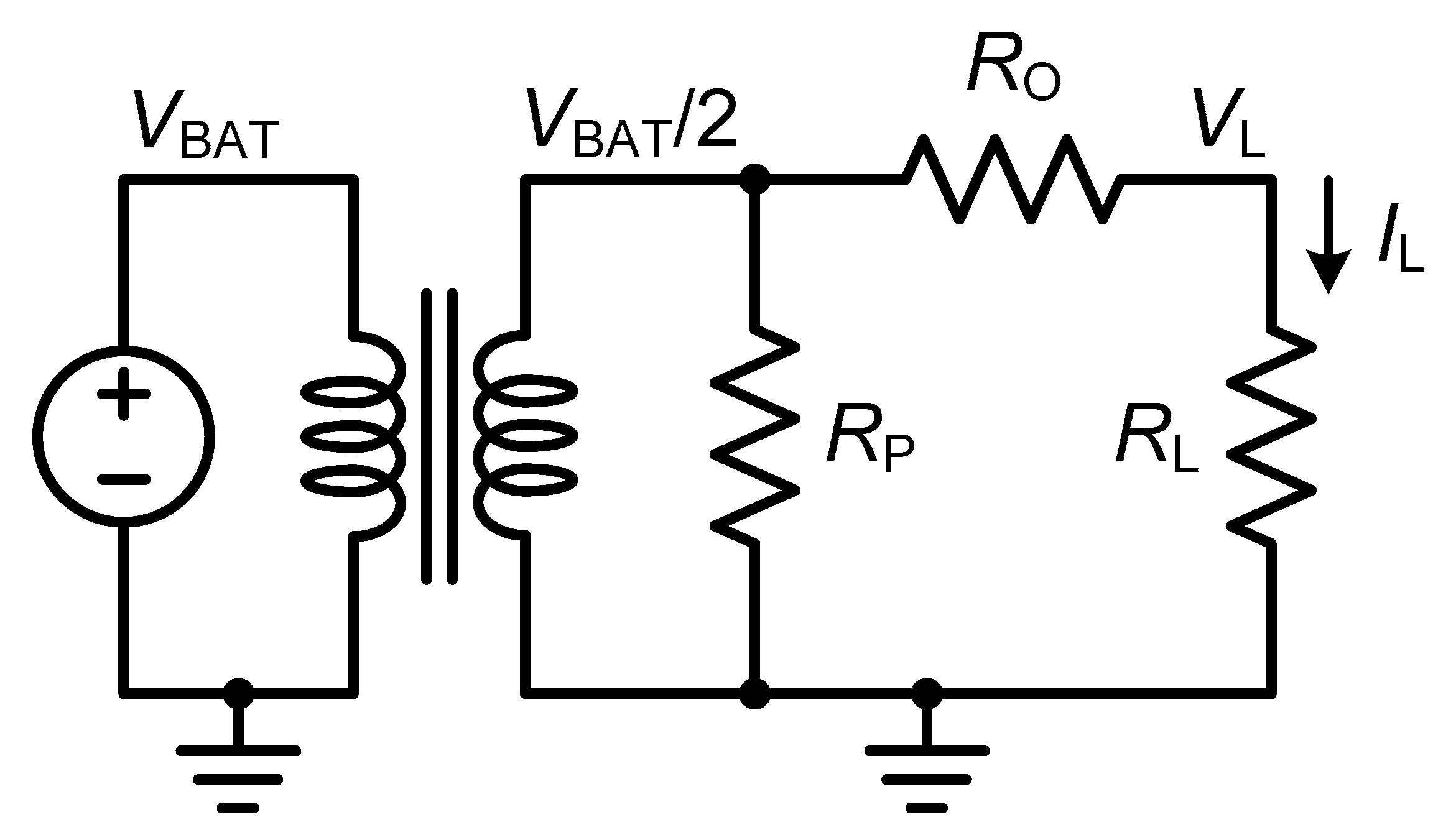
Figure 6 shows a simplified model of the 2:1 step-down SC DC–DC converter. The parallel resistor RP represents the shunt loss due to parasitic capacitances in the switches and flying capacitors. We note here that RP is independent of the output current. The output impedance RO is connected in series with the load resistor RL. RO changes the load voltage, and its power loss, called series loss, is the sum of the switch conductance loss and the intrinsic SC loss. The switch conductance loss is caused by the resistance in the on state of the switch. Increasing the size of the switch reduces the conductance loss but increases the shunt loss via the parasitic capacitance of the switch [23]. The intrinsic SC loss is caused by voltage ripple ΔVF due to the charge and discharge of the capacitor, as shown in Figure 5d. The intrinsic SC loss of a 2:1 step-down SC DC–DC converter can be expressed as [24,25]
where fSW denotes the switching frequency related to the two-phase operation. A fully-integrated SC DC–DC converter provides a relatively large load current with a small flying capacitance due to chip size limitations. Therefore, the intrinsic SC loss is larger than the switch conductance loss. In this paper, assuming an ideal switch, only the intrinsic SC loss is expressed as the series loss. Upon applying Equation (1) to this simplified model, the load current can be approximated as
The SC DC–DC converters regulate the output voltage via changing the value of Ro, which is adjusted through either frequency or pulse–width modulation of the switching clock.
2.2. Multiphase Interleaved SC DC–DC Converter for Low Switching Ripple
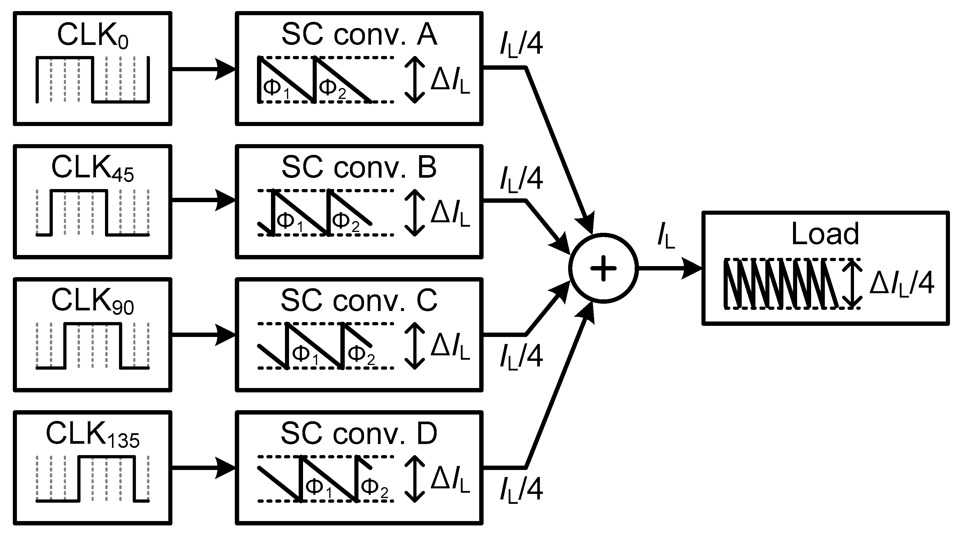
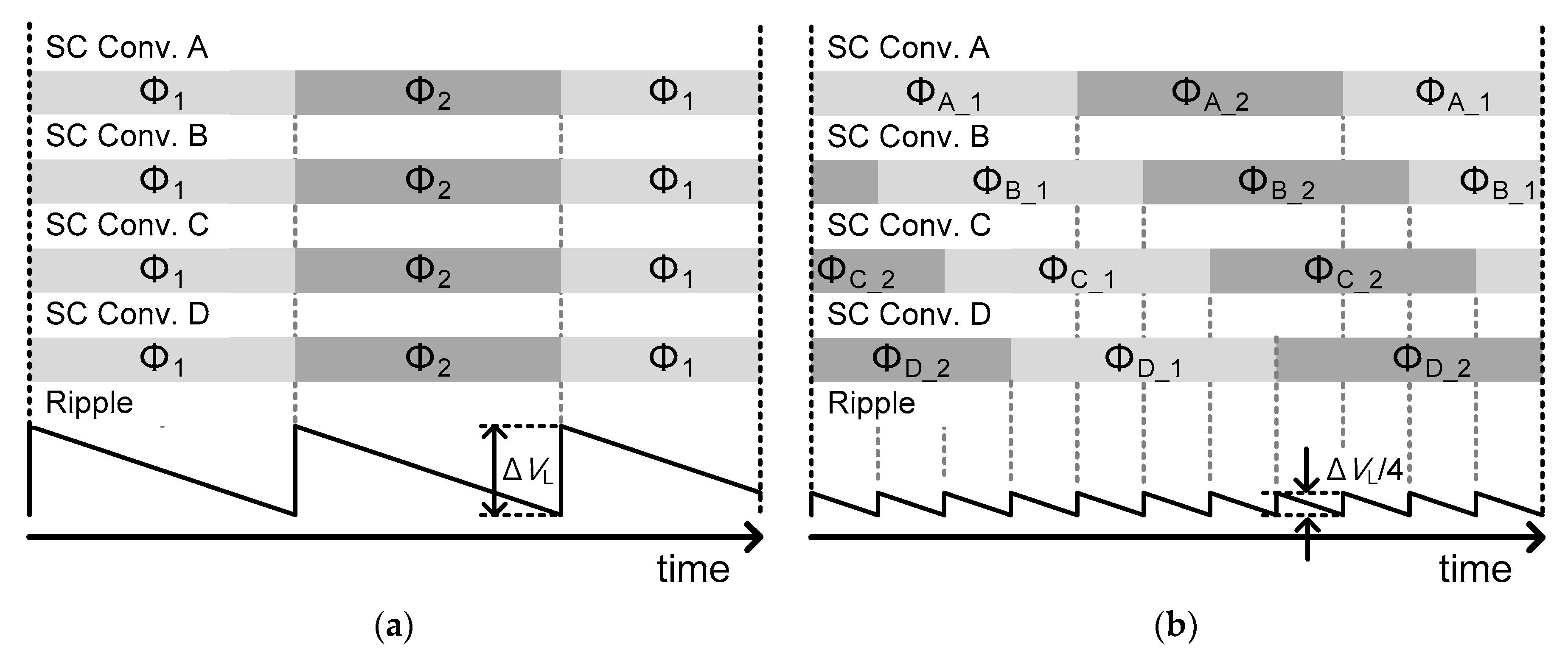
As the SC DC–DC converter performs repeated charging and discharging, the output voltage exhibits an inherent switching ripple. Multiphase interleaving aims to mitigate this ripple via dividing the converter into multiple units and driving each unit with different clock phases. Figure 7 illustrates a four-phase interleaved converter, with each unit utilizing a quarter of the total capacitance and operating at a 45° phase shift relative to the clocks of the neighboring nodes. The flying capacitances of all units are equal, and hence, the output charge per cycle is also identical. The output current of each unit is the same as that of the converter without interleaving. Thus, the charge flowing through each unit of the flying capacitor in multiphase interleaving is the same as that in the case of the original converter.
Figure 8 shows the operation of a four-phase interleaved SC DC–DC converter including the output voltage ripple with and without phase interleaving. In Figure 8a, each SC DC–DC converter without phase interleaving operates at the same clock phase (Φ1 and Φ2), producing output ripple ΔVL. In Figure 8b, each converter of the interleaving configuration operates with 45° phase-shifted clocks (ΦA_1, ΦB_1, ΦC_1, and ΦD_1). Therefore, the effective switching frequency fripple in the converter increases by a factor of four relative to the case with no interleaving, thereby reducing the output ripple to 25% of the original ΔVL. Multiphase interleaving reduces the voltage ripple by increasing the effective switching frequency but maintains switching losses. To mitigate the output voltage ripple, a load capacitor is generally used. Multiphase interleaving also decreases this load capacitor value by a factor of four due to the increased ripple frequency.
2.3. Output Voltage Regulation
The output voltage of the SC DC–DC converter can be modulated by the three methods depicted in Figure 9. First, frequency modulation enables the adjustment of the operating frequency of switching according to the load impedance, with the duty cycle usually set to 50%. This method changes the output impedance of the converter by varying the charge transferred from the flying capacitor to the load. However, it requires an additional voltage-controlled oscillator for frequency modulation. Second, time modulation enables the adjustment of the pulse width of the switching signal, which allows for control of the output current for the flying capacitors to charge or discharge. This method modulates the output current by varying the connection time to the output node. However, efficiency is low due to switching losses under light loads, given the low output current of the converter; nevertheless, the switching loss is maintained constant under this condition. Third, capacitance modulation of the charge transfer can be achieved by dividing the SC DC–DC converter into multiple converter cells in parallel and utilizing some cells to provide the required current to the load, thereby establishing “digital” operation. In this method, only the flying capacitors and switches of the converter cells involved in the output current circuit operate, thus improving the efficiency with respect to switching loss. However, the main limitation of this method is the required division of the SC DC–DC converter into cells for accurate output current control. This division increases the complexity of both the chip layout and the state machine to select the appropriate number of cells, thus imposing a tradeoff between efficiency and complexity.
2.4. DCpM Control
The DCpM approach allows control of the amount of flying capacitance associated with the charge transfer in the converter, thereby enabling load current regulation given that the amount of charge transferred in one clock cycle is proportional to this capacitance. With this method, the total switch size involved in the output current of the SC DC–DC converter can be adjusted according to the size of the flying capacitance. Thus, the shunt loss originating from parasitic capacitances of the flying capacitors and switches and the conduction loss due to the switch resistance are reduced when the load current is low, thereby maintaining high efficiency under light load.
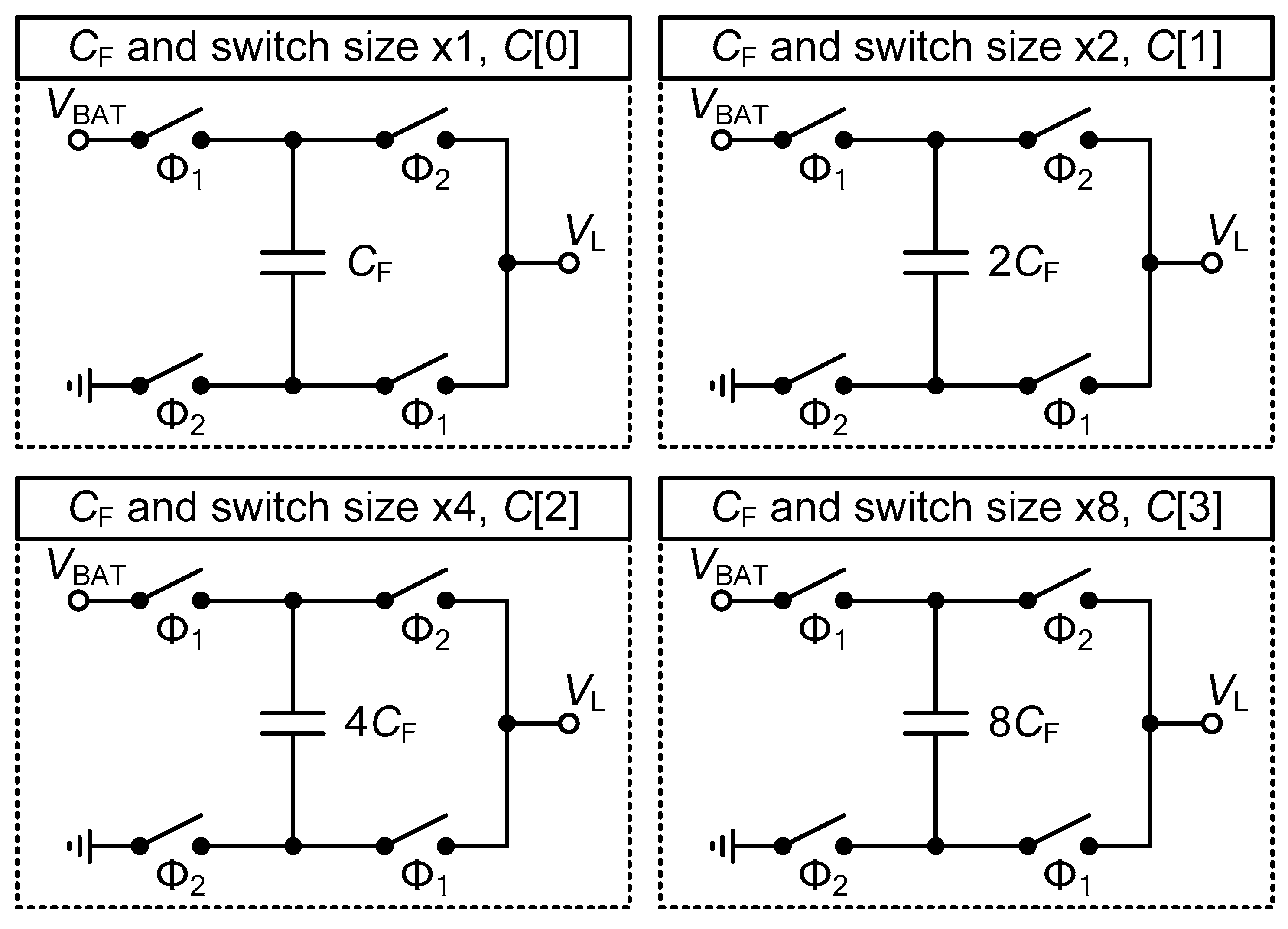
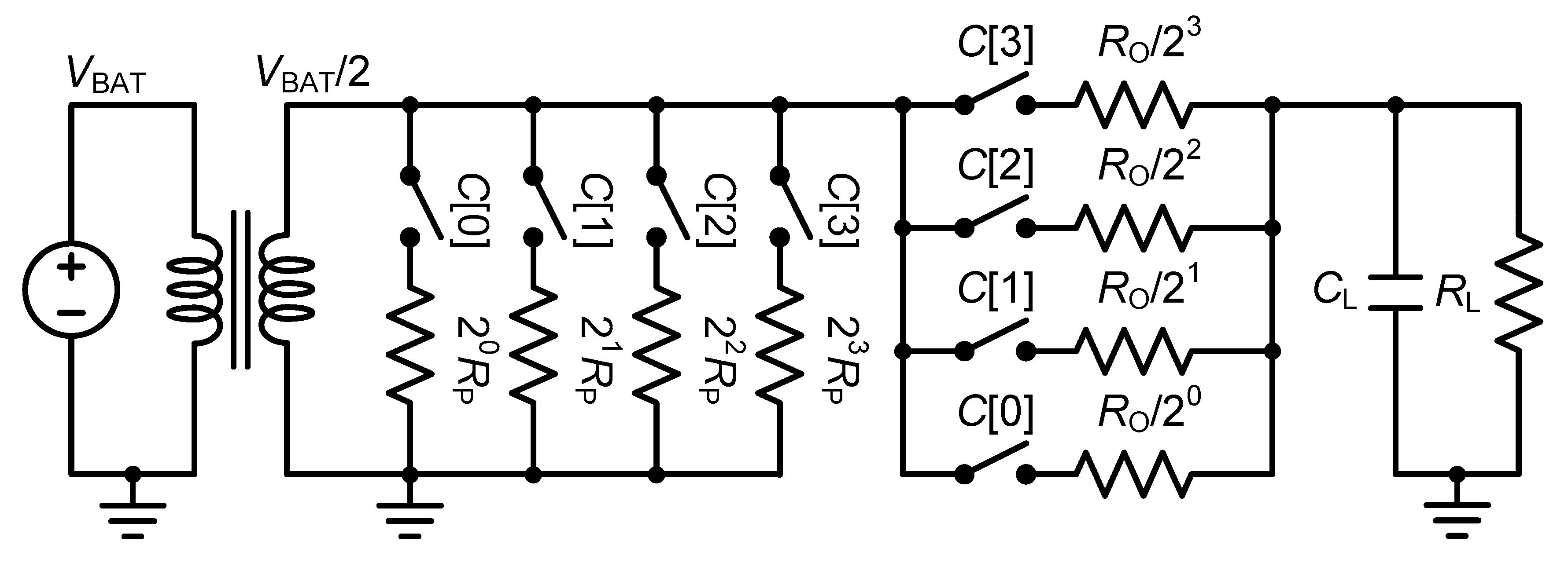
In the implementation of the SC DC–DC converter with DCpM control, the flying capacitor is divided into a binary-weight bank. Figure 10 shows the structure of the SC DC–DC converter with a four-bit DCpM control. The flying capacitance is divided into four different banks of size x1, x2, x4, and x8. These four converter cells form a single matrix, and the charge transfer operation is enabled by control code C[3:0]. Figure 11 shows a model of the proposed SC DC–DC converter based on a four-bit DCpM. The 2:1 transformer represents the required voltage step-down process. The output impedance RO and the shunt impedance RP are binary-weighted according to the DCpM control signal. The output impedance is determined as 1/(4·CF·fSW), where fSW and CF denote the switching frequency and the unit flying capacitance, respectively. The load current IL of the converter can be expressed as
where VI and VL represent the input and output voltages, respectively, and DCpM code C[n] determines the output current.
3. Proposed Low-Ripple SC DC–DC Converter
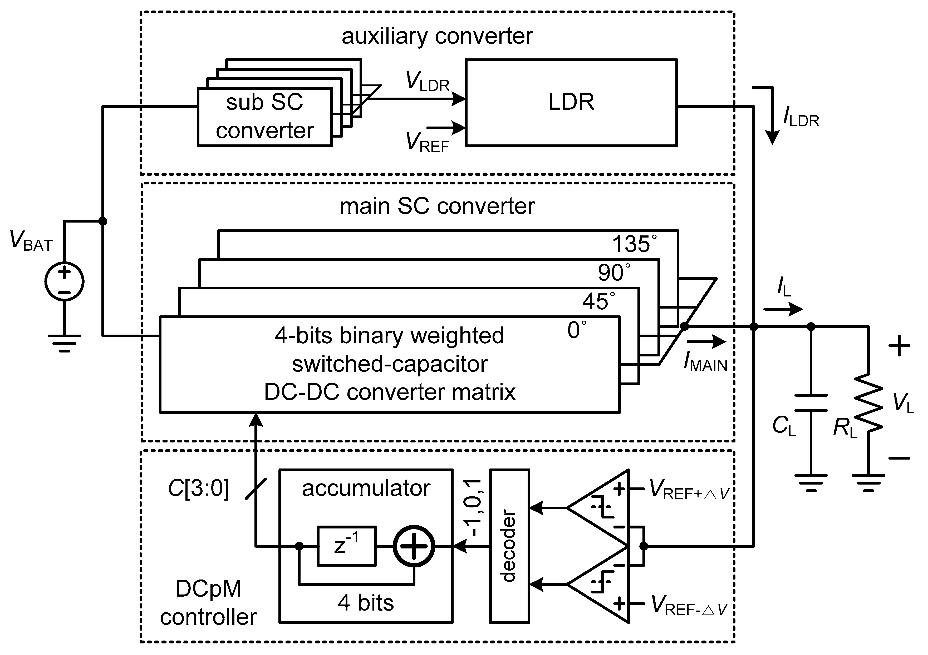
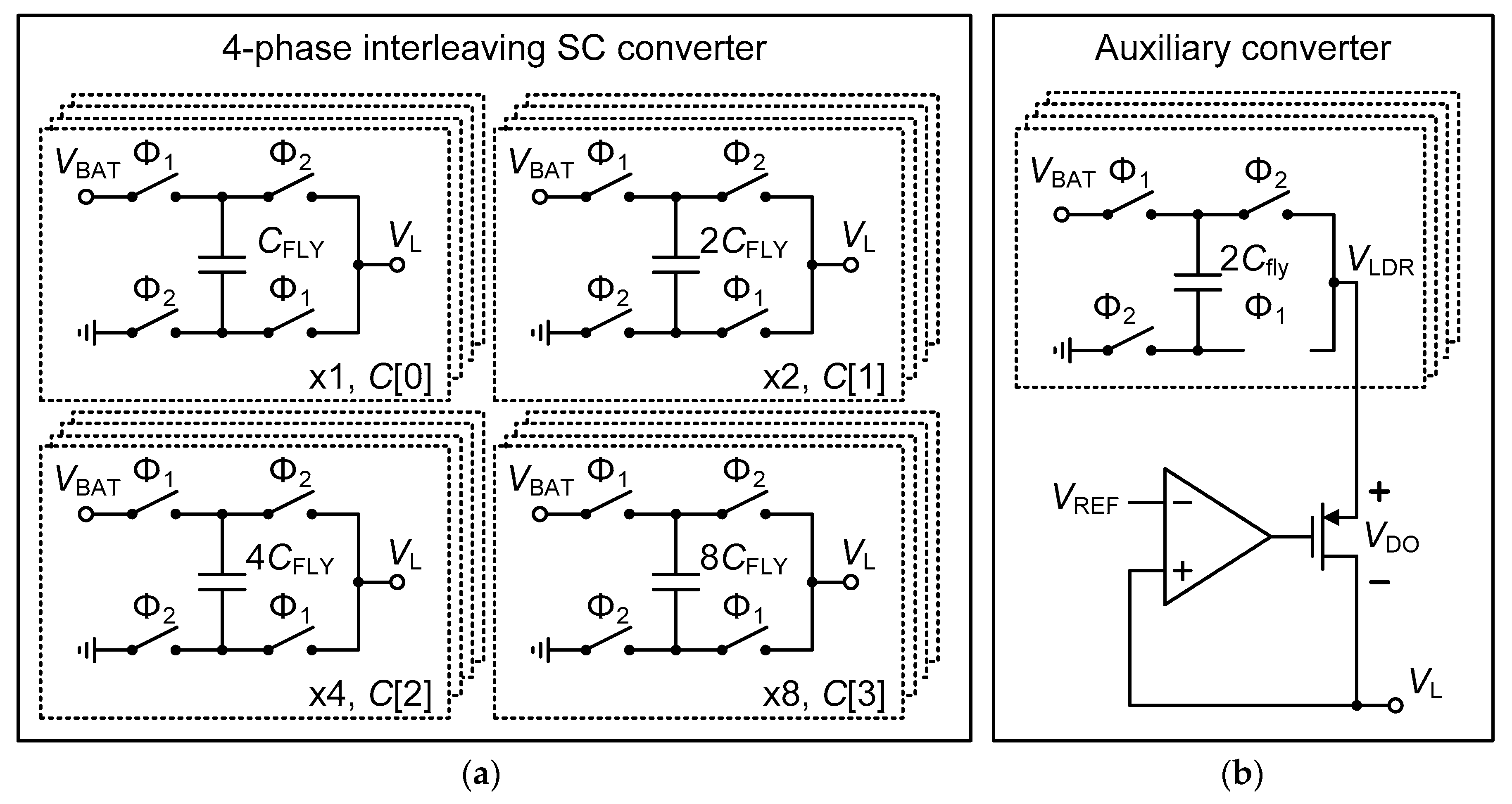
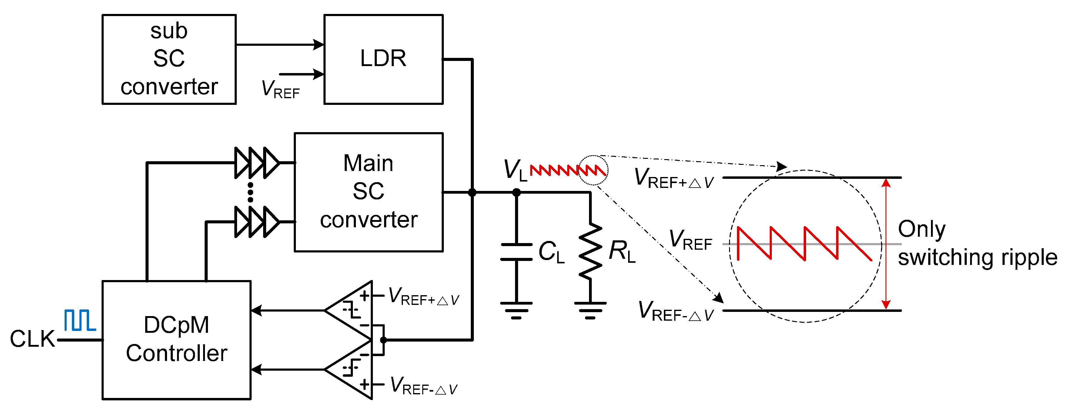
Figure 12 shows the block diagram of the proposed SC DC–DC converter, which is composed of a main converter, an auxiliary LDR, and a DCpM controller. The main converter provides most of the current to the load, whereas the LDR assists the main converter to provide an accurate output current. The LDR is powered by a small four-phase interleaved SC converter to improve efficiency. To reduce the switching ripple, four interleaved phases (0°, 45°, 90°, and 135°) are adopted for the SC DC–DC converter cells. The current of the main converter is controlled by the DCpM, which compares the output voltage with two reference voltages using two clocked comparators. If output voltage VO > VREF + ΔV or <VREF − ΔV, the binary code decreases or increases, respectively. If VL lies between VREF + ΔV and VREF − ΔV, the binary code remains unchanged.
Figure 13a shows one of the four-phase interleaved SC DC–DC converter matrices used in the main converter, which is composed of four converter cells. Each cell employs a 2:1 step-down topology and operates in a bi-phase mode (Φ1 and Φ2) with 50% duty cycle. The magnitudes of the flying capacitors CF and switches are four-bit binary-weighted. Binary code C[3:0] of the DCpM controller either enables or disables the operation of each converter cell to adjust the output current. As shown in Figure 13b, the auxiliary LDR powered by the small four-phase SC converter employs a p–channel metal–oxide–semiconductor (PMOS) pass transistor and a two-stage operational amplifier. Figure 14 shows the block diagram of the proposed LDR-assisted SC DC–DC converter with a low output ripple. The proposed converter exhibits only a switching ripple, and the main converter is controlled by the DCpM via two-boundary hysteresis feedback, which also produces a low-frequency control ripple. Nevertheless, the two-boundary controller can limit the control ripple between VREF − ∆V and VREF + ∆V. Therefore, the LDR with a low output current capability can compensate for the output current fluctuation due to the feedback control ripple by providing an opposite-phase accurate current to the load. This approach ensures that the DCpM control bits performing coarse tuning are fixed at every output current range, and hence, the output voltage ripple of the proposed converter presents no control ripple due to hysteresis feedback but only switching ripple.
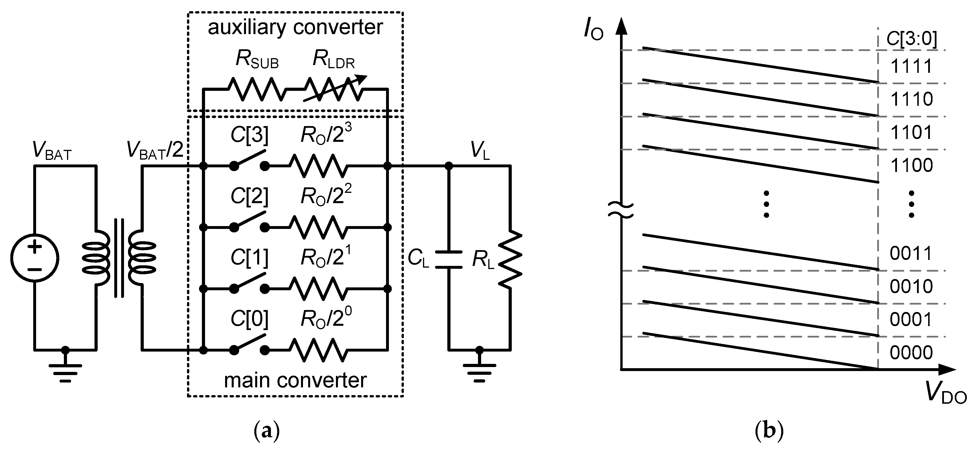
Figure 15a shows a simplified model of the proposed SC DC–DC converter, where the 2:1 transformer represents the 2:1 voltage step-down process. The main converter is described using a binary-weighed unit-resistance RO, which equals 1/(4·CFLY·fSW), where fSW and CFLY represent the switching frequency and unit flying capacitance, respectively. Current IMAIN of the main SC DC–DC converter can be expressed as
where VI, VO, and ki denote the input voltage, output voltage, and number of interleaved phases, respectively. The auxiliary LDR is modeled as a fixed resistance RSUB for each SC DC–DC converter cell and a variable resistance RLDR for the LDR. Consequently, output current ILDR of the auxiliary LDR can be expressed as
where VDO represents the dropout voltage of the pass transistor in the LDR. Hence, the auxiliary LDR can finely adjust the output current. From Figure 15b, we note that the main converter provides a discrete coarse current that is determined by the DCpM code, whereas the auxiliary converter “fills” the discrete steps using the linear LDR. Thus, the proposed SC DC–DC converter can provide any output current in its operating range without requiring a complex pulse–width modulated or pulse–frequency modulated controller.
4. Results and Discussion
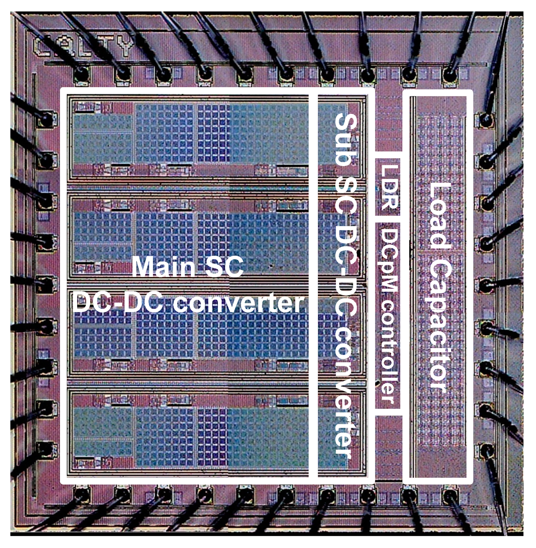
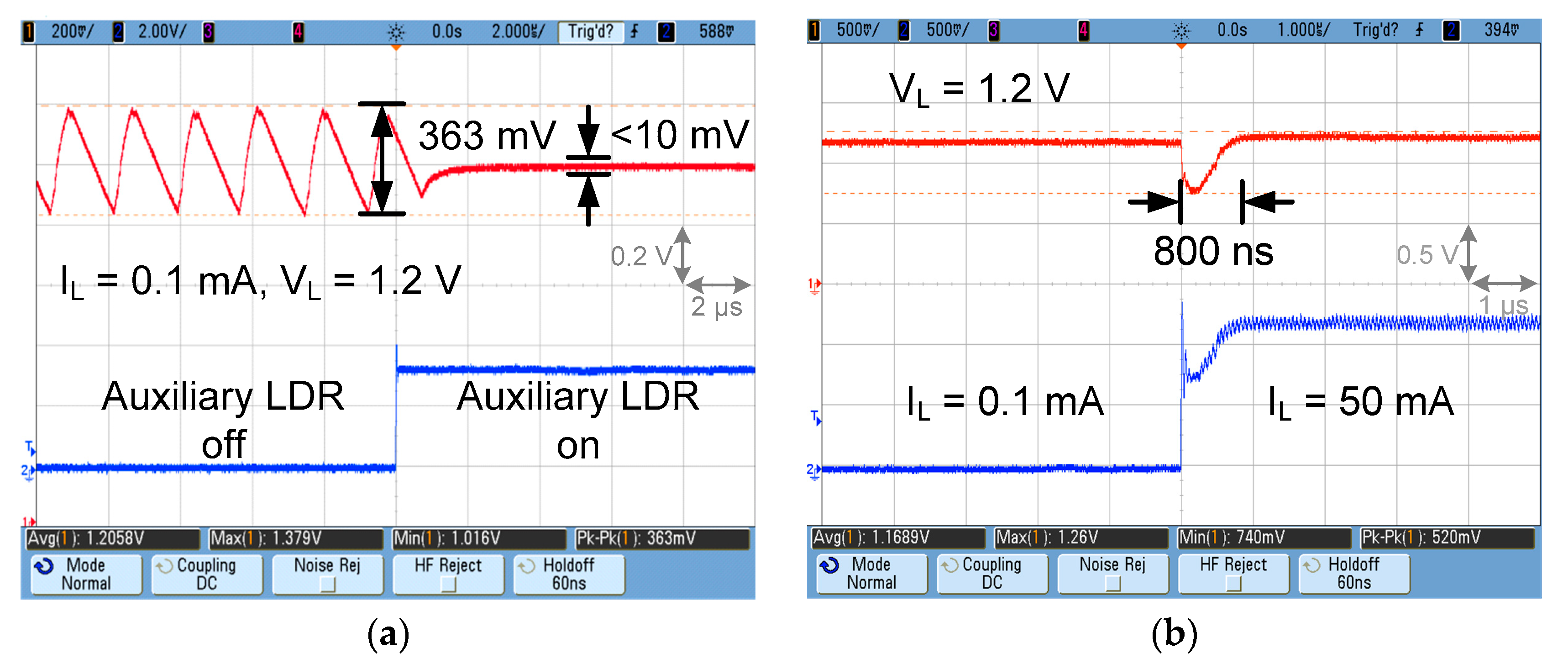
The proposed SC DC–DC converter was implemented using a 0.13 µm CMOS process (Dongbu HiTek, Seoul, Korea), which provides triple-well CMOS devices and MIM capacitors with eight metal layers and one poly layer. Figure 16 shows the microphotograph of the fabricated SC DC–DC converter. The core chip has an area of 2.04 mm2. Several pads are allocated to the input and output ports to reduce interconnection loss during measurement. The area of the capacitors is the major contributor to the size of the main SC DC–DC converter, converter cells, and load capacitor. Stacked capacitors utilizing the MIM and metal–oxide–semiconductor (MOS) capacitors are used to increase the capacitance per unit area, which are 1 fF/μm2 and 2.5 fF/μm2 for the MIM and MOS capacitors, respectively. Figure 17 shows the measured output voltage and current. The proposed converter has an output voltage range of 1.2 to 1.5 V from a 3.3 V supply. The output voltage waveforms were measured with the use of an MSO7104B oscilloscope (Keysight Technologies, Santa Rosa, CA, USA). The output voltage and LDR control signal are shown for the LDR in the on and off states in Figure 17a. The output voltage and current were set to 1.2 V and 100 μA, respectively. When the LDR was deactivated, a high ripple of approximately 380 mV was obtained. This is because the DCpM control code does not converge to one value at light loads, and the variation in the control code generates a large control ripple. However, the ripple drops below 10 mV upon activation of the LDR, which fine-tunes the output current and limits the DCpM control code to one value in the main SC DC–DC converter. Thus, the control ripple disappears due to the bounded DCpM control code, and only the switching ripple appears in the output voltage waveform. Figure 17b shows the load transient performance when the current suddenly changes from 120 µA to 50 mA. The output current and output voltage are restored to their regulated values in less than 800 ns.
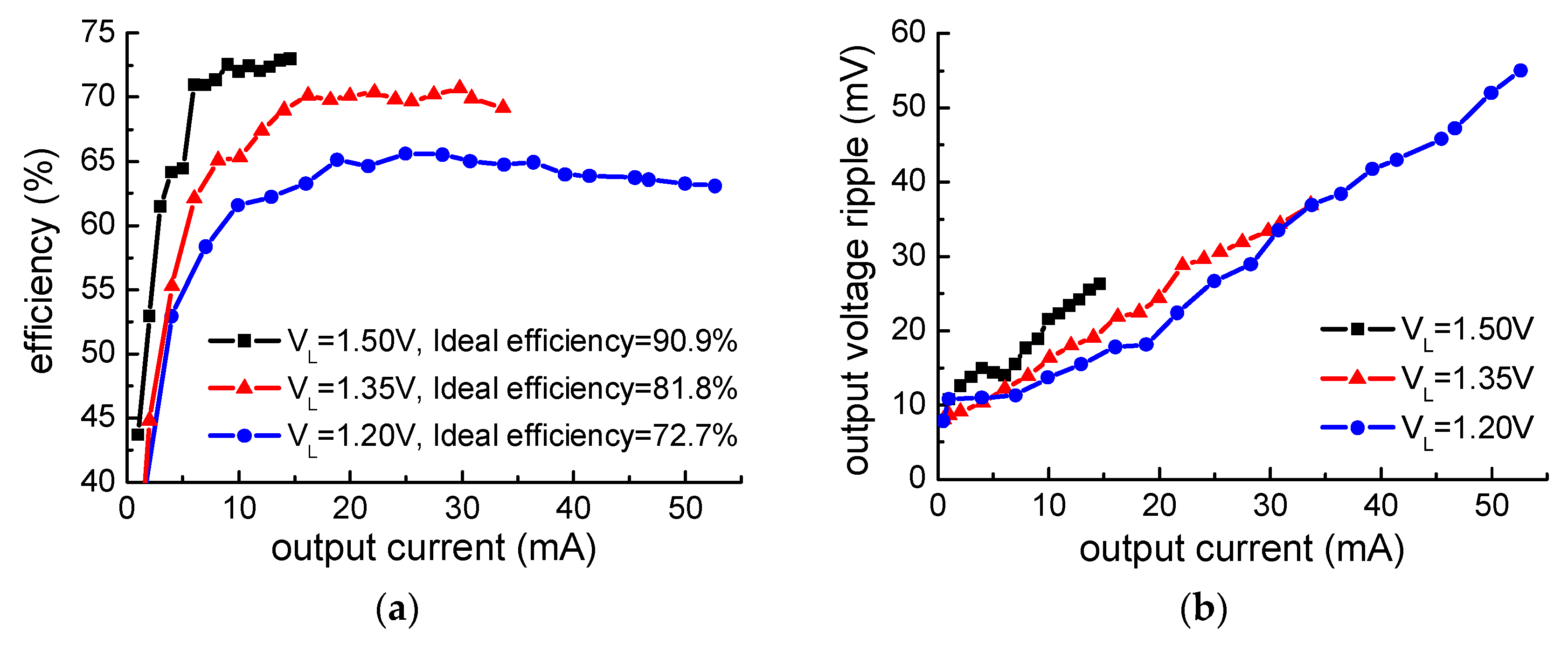
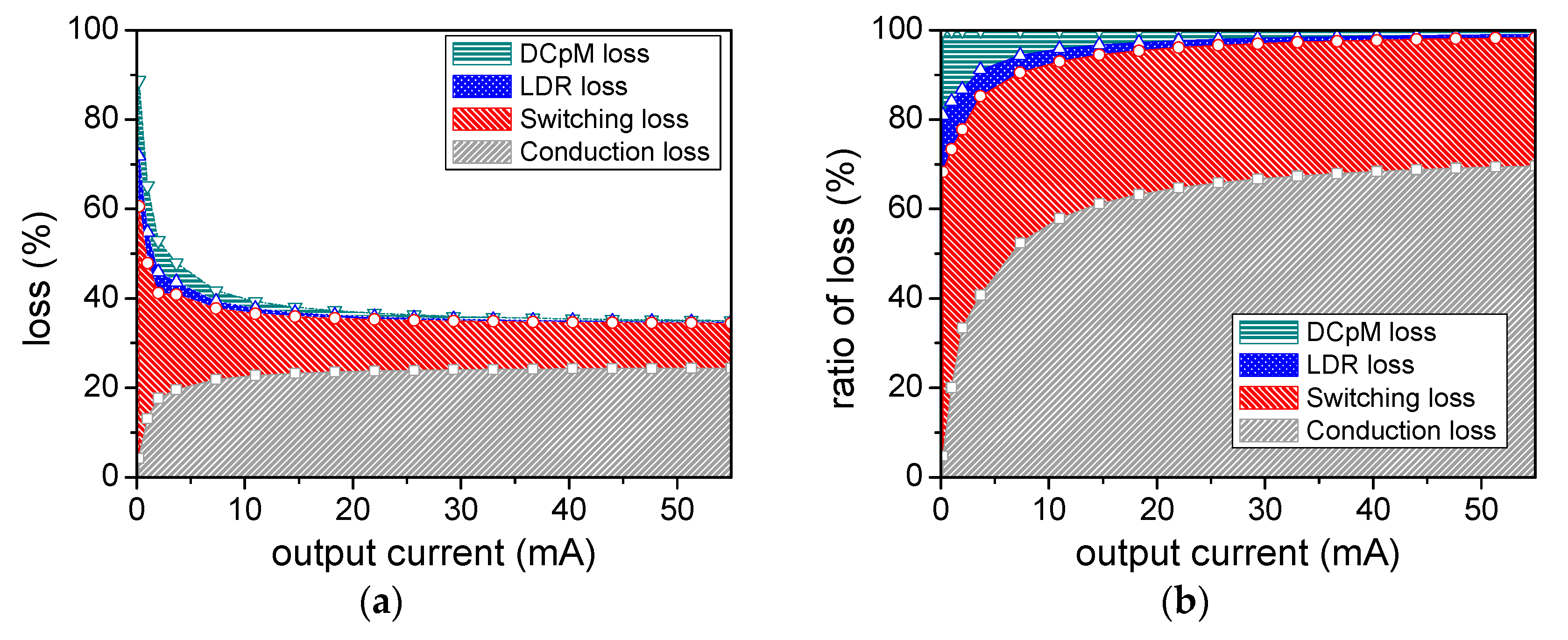
Figure 18a shows the measured efficiency according to the output current at the input voltage of 3.3 V. The efficiency depends on the output voltage, with the output voltage of 1.5 V corresponding to the highest efficiency and lowest output current. This is because the voltage ratio of the input to output is the closest to the transformer ratio of the 2:1 step-down topology in this case. The peak efficiency is 73, 70, and 65% at output voltages of 1.5, 1.35, and 1.2 V, respectively. Figure 18b shows the measured output voltage ripple according to the output current. The maximum ripple values remain below 26, 36, and 55 mV at output voltages of 1.5, 1.35, and 1.2 V, respectively. Figure 19 shows the loss contributions and their ratio according to the output current. At the very low output current, the DCpM loss and the LDR quiescent loss decrease the power efficiency, but as the current increases, the switching loss and conduction loss dominates. Figure 19a shows an efficiency reduction of 2.3% due to the LDR loss at the output current of 5 mA but only a 0.23% reduction at the output current of 53 mA.
Table 1 compares the performance of the proposed SC DC–DC converter with similar low-ripple converters. As the ripple depends on the output current, load capacitance, and switching frequency, we used the following figure of merit for a fair ripple comparison [26,27]:
As can be observed from the table, our approach affords the highest figure of merit.
5. Conclusions
We proposed a fully-integrated SC DC–DC converter with low ripple and high efficiency. The proposed converter employs a four-bit DCpM control and includes an auxiliary LDR in parallel. The DCpM efficiently optimizes the gate switching losses according to the output current, and a two-boundary hysteresis method supports the ripple control. In the proposed structure, the feedback ripple is removed by means of an auxiliary LDR connected in parallel. Moreover, four-phase interleaving is employed to reduce the switching ripple in the main converter. The proposed SC DC–DC converter affords an output voltage range of 1.2–1.5 V from a 3.3 V supply and achieves a peak efficiency of 73% and ripple below 55 mV over the entire output current range. We believe that our approach will find utility in power sources for sensor-based devices of the future.
Author Contributions
J.-Y.L., G.-S.K., and K.-I.O. carried out the experiments and computer simulation and wrote the paper under the supervision of D.B.
Funding
This research received no external funding.
Acknowledgments
This work was supported by the Institute for Information and Communications Technology Promotion (IITP) grant funded by the Korea government (MSIT) (No. 2018-0-01663, Development of Communication-Sensing Converged B5G Millimeter Wave System) and by the Chung-Ang University Graduate Research Scholarship in 2018.
Conflicts of Interest
The authors declare no conflict of interest.
References
- Su, W.; Wu, Z.; Fang, Y.; Bahr, R.; Raj, P.M.; Tummala, R.; Tentzeris, M.M. 3d printed wearable flexible SIW and microfluidics sensors for internet of things and smart health applications. In Proceedings of the 2017 IEEE MTT-S International Microwave Symposium (IMS), Honololu, HI, USA, 4–9 June 2017; pp. 544–547. [Google Scholar]
- Bang, S.; Blaauw, D.; Sylvester, D. A Successive-Approximation Switched-Capacitor DC–DC Converter With Resolution of VIN/2N for a Wide Range of Input and Output Voltages. IEEE J. Solid-State Circuits 2016, 51, 543–556. [Google Scholar]
- Saif, H.; Lee, Y.; Lee, H.; Kim, M.; Khan, M.; Chun, J.H.; Lee, Y. A Wide Load Current and Voltage Range Switched Capacitor DC–DC Converter with Load Dependent Configurability for Dynamic Voltage Implementation in Miniature Sensors. Energies 2018, 11, 3092. [Google Scholar] [CrossRef]
- Pei, C.; Booth, R.; Ho, H.; Kusaba, N.; Li, X.; Brodsky, M.; Iyer, S. A novel, low-cost deep trench decoupling capacitor for high-performance, low-power bulk CMOS applications. In Proceedings of the 2008 9th International Conference on Solid-State and Integrated-Circuit Technology, Beijing, China, 20–23 October 2008; pp. 1146–1149. [Google Scholar]
- Kudva, S.S.; Harjani, R. Fully-integrated on-chip DC-DC converter with a 450X output range. IEEE J. Solid-State Circuits 2011, 46, 1940–1951. [Google Scholar] [CrossRef]
- Ahsanuzzaman, S.M.; Prodić, A.; Johns, D.A. An integrated high-density power management solution for portable applications based on a multioutput switched-capacitor circuit. IEEE Trans. Power Electron. 2016, 31, 4305–4323. [Google Scholar] [CrossRef]
- Zimmer, B.; Lee, Y.; Puggelli, A.; Kwak, J.; Jevtić, R.; Keller, B.; Bailey, S.; Blagojević, M.; Chiu, P.F.; Le, H.P.; et al. A RISC-V vector processor with simultaneous-switching switched-capacitor DC–DC converters in 28 nm FDSOI. IEEE J. Solid-State Circuits 2016, 51, 930–942. [Google Scholar]
- Sung, E.T.; Park, S.; Baek, D. A Fast-Transient Output Capacitor-Less Low-Dropout Regulator Using Active-Feedback and Current-Reuse Feedforward Compensation. Energies 2018, 11, 688. [Google Scholar] [CrossRef]
- Lu, Y.; Jiang, J.; Ki, W.H. Design Considerations of Distributed and Centralized Switched-Capacitor Converters for Power Supply On-Chip. IEEE J. Emerg. Sel. Top. Power Electron. 2018, 6, 515–525. [Google Scholar] [CrossRef]
- Dini, M.; Romani, A.; Filippi, M.; Tartagni, M. A nanocurrent power management IC for low-voltage energy harvesting sources. IEEE Trans. Power Electron. 2016, 31, 4292–4304. [Google Scholar] [CrossRef]
- Avalur, K.K.G.; Azeemuddin, S. A 6–18 V hybrid power management IC with adaptive dropout for improved system efficiency up to 150 °C. IEEE J. Emerg. Sel. Top. Power Electron. 2018, 6, 477–484. [Google Scholar] [CrossRef]
- Wibben, J.; Harjani, R. A high-efficiency DC–DC converter using 2 nH integrated inductors. IEEE J. Solid-State Circuits 2008, 43, 844–854. [Google Scholar] [CrossRef]
- Li, Q.; Dong, Y.; Lee, F.C.; Gilham, D.J. High-density low-profile coupled inductor design for integrated point-of-load converters. IEEE Trans. Power Electron. 2013, 28, 547–554. [Google Scholar] [CrossRef]
- Chang, L.; Montoye, R.K.; Ji, B.L.; Weger, A.J.; Stawiasz, K.G.; Dennard, R.H. A fully-integrated switched-capacitor 2∶1 voltage converter with regulation capability and 90% efficiency at 2.3 A/mm2. In Proceedings of the 2010 Symposium on VLSI Circuits, Honolulu, HI, USA, 16–18 June 2010; pp. 55–56. [Google Scholar]
- Ramadass, Y.K.; Fayed, A.A.; Chandrakasan, A.P. A fully-integrated switched-capacitor step-down DC-DC converter with digital capacitance modulation in 45 nm CMOS. IEEE J. Solid-State Circuits 2010, 45, 2557–2565. [Google Scholar] [CrossRef]
- Lee, H.; Mok, P.K. An SC voltage doubler with pseudo-continuous output regulation using a three-stage switchable opamp. IEEE J. Solid-State Circuits 2007, 42, 1216–1229. [Google Scholar] [CrossRef]
- Calhoun, B.H.; Chandrakasan, A.P. Ultra-dynamic voltage scaling (UDVS) using sub-threshold operation and local voltage dithering. IEEE J. Solid-State Circuits 2006, 41, 238–245. [Google Scholar] [CrossRef]
- Sanders, S.R.; Alon, E.; Le, H.P.; Seeman, M.D.; John, M.; Ng, V.W. The road to fully integrated DC–DC conversion via the switched-capacitor approach. IEEE Trans. Power Electron. 2013, 28, 4146–4155. [Google Scholar] [CrossRef]
- Le, H.P.; Sanders, S.R.; Alon, E. Design techniques for fully integrated switched-capacitor DC-DC converters. IEEE J. Solid-State Circuits 2011, 46, 2120–2131. [Google Scholar] [CrossRef]
- Shenoy, P.S.; Amaro, M.; Morroni, J.; Freeman, D. Comparison of a buck converter and a series capacitor buck converter for high-frequency, high-conversion-ratio voltage regulators. IEEE Trans. Power Electron. 2016, 31, 7006–7015. [Google Scholar] [CrossRef]
- Jain, R.; Kim, S.T.; Vaidya, V.; Ravichandran, K.; Tschanz, J.W.; De, V. Conductance modulation techniques in switched-capacitor DC-DC converter for maximum-efficiency tracking and ripple mitigation in 22 nm tri-gate CMOS. IEEE J. Solid-State Circuits 2015, 50, 1809–1819. [Google Scholar] [CrossRef]
- Kudva, S.S.; Harjani, R. Fully Integrated Capacitive DC–DC Converter with All-Digital Ripple Mitigation Technique. IEEE J. Solid-State Circuits 2013, 48, 1910–1920. [Google Scholar] [CrossRef]
- Jeon, H.; Kim, K.K.; Kim, Y.B. Fully Integrated on-Chip Switched DC–DC Converter for Battery-Powered Mixed-Signal SoCs. Symmetry 2017, 9, 18. [Google Scholar] [CrossRef]
- Seeman, M.D.; Sanders, S.R. Analysis and optimization of switched-capacitor DC–DC converters. IEEE Trans. Power Electron. 2008, 23, 841–851. [Google Scholar] [CrossRef]
- Butzen, N.; Steyaert, M.S. Scalable parasitic charge redistribution: Design of high-efficiency fully integrated switched-capacitor DC–DC converters. IEEE J. Solid-State Circuits 2016, 51, 2843–2853. [Google Scholar] [CrossRef]
- Van Breussegem, T.; Steyaert, M. A 82% efficiency 0.5% ripple 16-phase fully integrated capacitive voltage doubler. In Proceedings of the 2009 Symposium on VLSI Circuits, Kyoto, Japan, 16–18 June 2009; pp. 198–199. [Google Scholar]
- Yoo, A.; Chang, M.; Trescases, O.; Wang, H.; Ng, W.T. FOM (Figure of Merit) Analysis for Low Voltage Power MOSFETs in DC-DC Converter. Proc. IEEE Conf. Electron Devices Solid-State Circuits 2007, 1039–1042. [Google Scholar]
- Lisboa, P.C.; Pérez-Nicoli, P.; Veirano, F.; Silveira, F. General top/bottom-plate charge recycling technique for integrated switched capacitor DC-DC converters. IEEE Trans. Circuits Syst. I 2016, 63, 470–481. [Google Scholar] [CrossRef]
Figure 1.
Types of sensor modules: (a) Sensor module with multichip architecture and (b) fully integrated sensor module (PMIC, power management IC; PMU, power management unit; and LDO, linear low dropout regulator).
Figure 1.
Types of sensor modules: (a) Sensor module with multichip architecture and (b) fully integrated sensor module (PMIC, power management IC; PMU, power management unit; and LDO, linear low dropout regulator).

Figure 2.
Configuration of the step-down switching DC–DC converters: (a) Inductor-based converter and (b) capacitor-based converter.
Figure 2.
Configuration of the step-down switching DC–DC converters: (a) Inductor-based converter and (b) capacitor-based converter.

Figure 3.
Block diagram of the switched-capacitor (SC) DC–DC converter using one-boundary hysteresis feedback and its output ripple voltage.
Figure 3.
Block diagram of the switched-capacitor (SC) DC–DC converter using one-boundary hysteresis feedback and its output ripple voltage.

Figure 4.
Ripple mitigation techniques.

Figure 5.
Operation of a step-down SC DC–DC converter. (a) Block diagram of a 2:1 step-down SC DC–DC converter; (b) operation during phase 1; (c) operation during phase 2; and (d) the output voltage ripple.
Figure 5.
Operation of a step-down SC DC–DC converter. (a) Block diagram of a 2:1 step-down SC DC–DC converter; (b) operation during phase 1; (c) operation during phase 2; and (d) the output voltage ripple.

Figure 6.
Simplified model of a 2:1 step-down switched-capacitor (SC) DC–DC converter.

Figure 7.
Block diagram of s four-phase interleaved SC DC–DC converter.

Figure 8.
Operation of an interleaved switched-capacitor (SC) DC–DC converter: (a) Without interleaving and (b) upon applying interleaving.
Figure 8.
Operation of an interleaved switched-capacitor (SC) DC–DC converter: (a) Without interleaving and (b) upon applying interleaving.

Figure 9.
Methods for output voltage regulation: (a) Pulse–frequency modulation; (b) pulse–width modulation; and (c) capacitance modulation.
Figure 9.
Methods for output voltage regulation: (a) Pulse–frequency modulation; (b) pulse–width modulation; and (c) capacitance modulation.

Figure 10.
Binary-weighted switched-capacitor (SC) DC–DC converter cells for DCpM.

Figure 11.
Model of the proposed switched-capacitor (SC) DC–DC converter using a four-bit DCpM.

Figure 12.
Block diagram of the proposed switched-capacitor (SC) DC–DC converter.

Figure 13.
Schematic of (a) the main switched-capacitor (SC) DC–DC converter and (b) the auxiliary SC DC–DC converter.
Figure 13.
Schematic of (a) the main switched-capacitor (SC) DC–DC converter and (b) the auxiliary SC DC–DC converter.

Figure 14.
Block diagram of the proposed LDR-assisted SC DC–DC converter and its output ripple voltage.
Figure 14.
Block diagram of the proposed LDR-assisted SC DC–DC converter and its output ripple voltage.

Figure 15.
(a) The simplified model of the proposed switched-capacitor (SC) DC–DC converter and (b) output current versus dropout voltage of the LDR pass transistor.
Figure 15.
(a) The simplified model of the proposed switched-capacitor (SC) DC–DC converter and (b) output current versus dropout voltage of the LDR pass transistor.

Figure 16.
Microphotograph of the proposed switched-capacitor (SC) converter.

Figure 17.
Measured output voltage and current waveforms: (a) the ripple voltage at a low output current with and without the low dropout regulator (LDR) in operation and (b) the load transient responses to a sudden current variation.
Figure 17.
Measured output voltage and current waveforms: (a) the ripple voltage at a low output current with and without the low dropout regulator (LDR) in operation and (b) the load transient responses to a sudden current variation.

Figure 18.
(a) Measured efficiency and (b) voltage ripple according to output current.

Figure 19.
Loss contributions from DCpM, LDR, switching, and conduction losses versus output current for VL = 1.2 V: (a) the loss contributions and (b) the ratio of loss contribution.
Figure 19.
Loss contributions from DCpM, LDR, switching, and conduction losses versus output current for VL = 1.2 V: (a) the loss contributions and (b) the ratio of loss contribution.


Table 1.
Comparison of results of previously reported studies and current study.
| Characteristic | [15] | [22] | [26] | [28] | This Work |
|---|---|---|---|---|---|
| Technology (nm) | 45 | 130 | 130 | 130 | 130 |
| Input voltage (V) | 1.8 | 1.8 | 1–1.2 | 1.2 | 3.3 |
| Output voltage (V) | 0.8–1 | 0.3–0.55 | 1.8–2.1 | 0.2–1.1 | 1.2–1.5 |
| Maximum load current (mA) | 10 | 55 | 2.61 | 2.53 | 53 |
| Power density (mW/mm2) | 50 | 24.5 | 0.67 | 7.56 | 31.2 |
| Flying capacitance (pF) | 534 | - | 400 | 840 | 2176 |
| Load capacitance (pF) | 700 | 5000 | 400 | 764 | 1000 |
| Ripple (mV) | <50 | <50 | <10 | 30 @IL = 30 μA | 8–55 |
| Peak efficiency (%) | 69 | 70 | 82 | 80.6 | 73 |
| Switching frequency (MHz) | 30 | 100 | 20 | 5 | 40 |
| Figure of merit, Equation (6) | 9.5 | 2.2 | 14 | 3.25 | 24.1 |
| Active area (mm2) | 0.16 | 0.97 | 2.25 | 0.291 | 2.04 |
© 2019 by the authors. Licensee MDPI, Basel, Switzerland. This article is an open access article distributed under the terms and conditions of the Creative Commons Attribution (CC BY) license (http://creativecommons.org/licenses/by/4.0/).
Share and Cite
MDPI and ACS Style
Lee, J.-Y.; Kim, G.-S.; Oh, K.-I.; Baek, D. Fully Integrated Low-Ripple Switched-Capacitor DC–DC Converter with Parallel Low-Dropout Regulator. Electronics 2019, 8, 98. https://doi.org/10.3390/electronics8010098
AMA Style
Lee J-Y, Kim G-S, Oh K-I, Baek D. Fully Integrated Low-Ripple Switched-Capacitor DC–DC Converter with Parallel Low-Dropout Regulator. Electronics. 2019; 8(1):98. https://doi.org/10.3390/electronics8010098
Chicago/Turabian StyleLee, Jeong-Yun, Gwang-Sub Kim, Kwang-Il Oh, and Donghyun Baek. 2019. "Fully Integrated Low-Ripple Switched-Capacitor DC–DC Converter with Parallel Low-Dropout Regulator" Electronics 8, no. 1: 98. https://doi.org/10.3390/electronics8010098
Note that from the first issue of 2016, this journal uses article numbers instead of page numbers. See further details here.