Performance Evaluation of a Semi-Dual-Active-Bridge with PPWM Plus SPS Control


Faculty of Information Technology, Macau University of Science and Technology, Taipa, Macau 999078, China
*
Author to whom correspondence should be addressed.
Electronics 2018, 7(9), 184; https://doi.org/10.3390/electronics7090184
Submission received: 24 August 2018
/
Revised: 5 September 2018
/
Accepted: 7 September 2018
/
Published: 9 September 2018
(This article belongs to the Special Issue Applications of Power Electronics)
Abstract
:In this paper, a semi-dual-active-bridge (S-DAB) DC/DC converter with primary pulse-width modulation plus secondary phase-shifted (PPWM + SPS) control for boost conversion is analyzed in detail. Under the new control scheme, all effective operation modes are identified at first. Then, the working principle, switching behaviour, and operation range in each mode are discussed. Compared with conventional secondary phase-shifted control, PPWM + SPS control with two controllable phase-shift angles can extend the zero-voltage switching (ZVS) range and enhance control flexibility. In addition, an effective control route is also given that can make the converter achieve at the global minimum root-mean-square (RMS) current across the whole power range and avoid the voltage ringing on the transformer secondary-side at a light load. Finally, a 200 W prototype circuit is built and tested to verify correctness and effectiveness of theoretical results.
1. Introduction
With the development of modern technology, there is a constant rise in energy use. Therefore, the concerns regarding the availability of fossil energy and the associated pollution in the mining and consumption process is continuously growing too. In order to alleviate the energy crisis and environmental pollution, the use of renewable energy (solar energy, wind energy, etc.) has developed rapidly around the world. As an important component for the application of renewable energy, the DC/DC converter with higher performance has been one of the most popular research fields [1,2,3,4,5]. So far, a number of DC/DC converter topologies have been proposed according to the various application requirements. In these converters, the phase-shift full-bridge converter is more attractive due to high power density, electrical isolation, easy to realize soft-switching commutation, high efficiency and low electromagnetic interference (EMI) [6,7,8,9,10,11,12,13]. However, it still suffers from high voltage ringing, reverse recovery on the secondary-side rectifier diodes, limited zero-voltage switching (ZVS) range and duty cycle loss.
To extend the ZVS range, a series of the full-bridge converters with various resonant tanks are presented. Among them, the converters with LC or LLC resonant tank are more attractive [14,15,16,17,18,19]. Nevertheless, the parameters of resonant tank should be selected carefully to achieve higher performance. Meanwhile, the design of magnetic components becomes complicated. On the other hand, when the phase-shift full-bridge converter works at high-output voltage and high-power case, the reverse-recovery problem of the rectifier diodes becomes more serious. In order to solve this problem, two active switches are introduced into the secondary-side rectifier of the converter, which is named the semi-dual-active-bridge (S-DAB) converter [20,21,22]. On this basis, two modified S-DAB topologies in [23,24] are proposed to only reduce the voltage stress on primary-side and secondary-side semiconductor devices, respectively. Furthermore, the S-DAB converter with an LC resonant tank is also presented in [25,26]. However, when the S-DAB converters work in a discontinuous-current mode (DCM) for boost operation, the voltage ringing phenomenon is generated on the transformer secondary-side. In particular, at the high switching frequency, high power and voltage levels, the excessive ringing might result in strong EMI, distorted gating signals and abnormal high peak voltages across the switches. In addition, the amount of power loss from snubber/parasitic capacitor will also increase during the ringing process [27,28]. Although a customized RC snubber is helpful to alleviate this problem, extra loss will be introduced in continuous-current mode (CCM) operation and the overall efficiency would be lower.
To the authors’ best knowledge, the voltage ringing problem in S-DAB has yet to be resolved. In this paper, PPWM + SPS control is applied on an S-DAB converter for boost operation to further improve performance, which also avoids the voltage ringing problem. The rest of this paper is organized as follows: in Section 2, each steady-sate mode of an S-DAB converter with PPWM + SPS control is analyzed comprehensively, including working principle, switching behaviour, and operation range. In Section 3, an effective control route across the whole power range is presented in order to achieve minimum root-mean-square (RMS) current and no voltage ringing. Experimental results are provided in Section 4. Conclusions are drawn in Section 5.
2. Operation Principle of an S-DAB Converter with PPWM + SPS Control
2.1. Basic Operation Principle
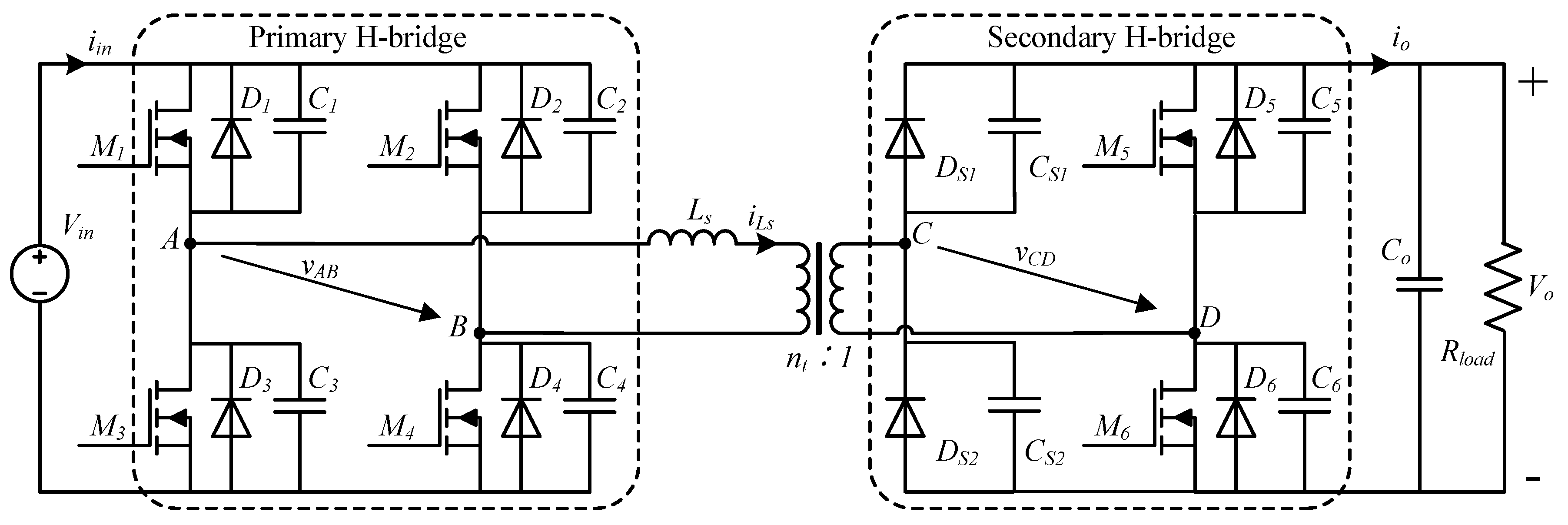
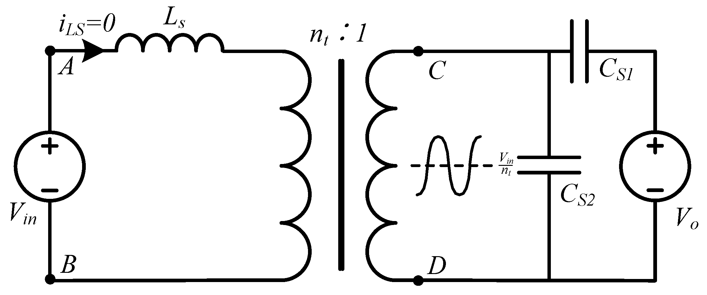
The schematic of an S-DAB converter is shown in Figure 1. The primary H-bridge consists of four switches (), while the secondary H-bridge is realized by a diode leg ( and ) and a switch leg ( and ). The high frequency transformer T with a turns ratio of not only provides galvanic isolation, but also matches voltage level. The voltage gain is defined as , and refers to boost operation. The inductor includes the leakage inductance of the transformer and an external inductance. The filter capacitor is connected in parallel with the load to depress the output voltage ripple. In this paper, PPWM + SPS control with two phase shift angles is employed on an S-DAB converter. All switches operate at the same frequency with 50% duty cycle, and switches in each switch leg are turned on/off complementarily. is defined as the inner phase-shift by which the gating signal of lags that of . Similarly, is defined as the outer-phase-shift by which the gating signal of lags that of . Two pulse-width-modulated voltages and are generated by the two bridges, respectively. The pulse-width of is determined by solely. However, the waveform of is associated with not only phase-shift angles but also the load level.
Depending on the relationship between two phase-shifts, an S-DAB converter with PPWM + SPS control can operate in three steady-state working modes, including one CCM (Mode A) and two DCMs, (Mode B and C). In the following part, each mode will be analyzed in detail one by one. In order to simplify the analysis process, four assumptions are made as follows:
- All components, such as switches, diodes are ideal and lossless.
- The magnetizing inductance of the transformer is infinity.
- The snubber/parasitic capacitors and dead-times influence are neglected.
- The filter capacitor is large enough to maintain constant voltage on the load.
2.2. Steady-State Analysis of Continuous-Current Mode
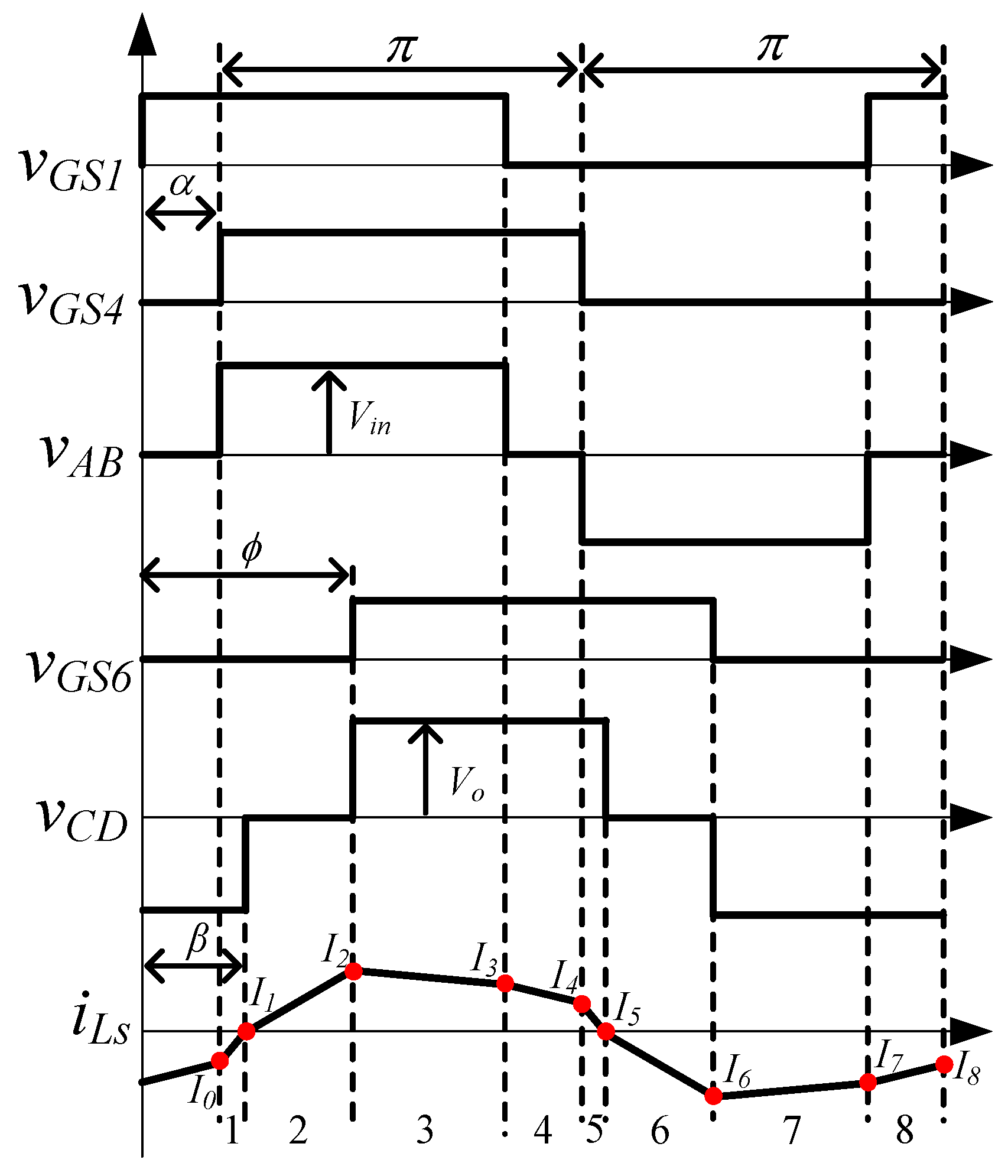
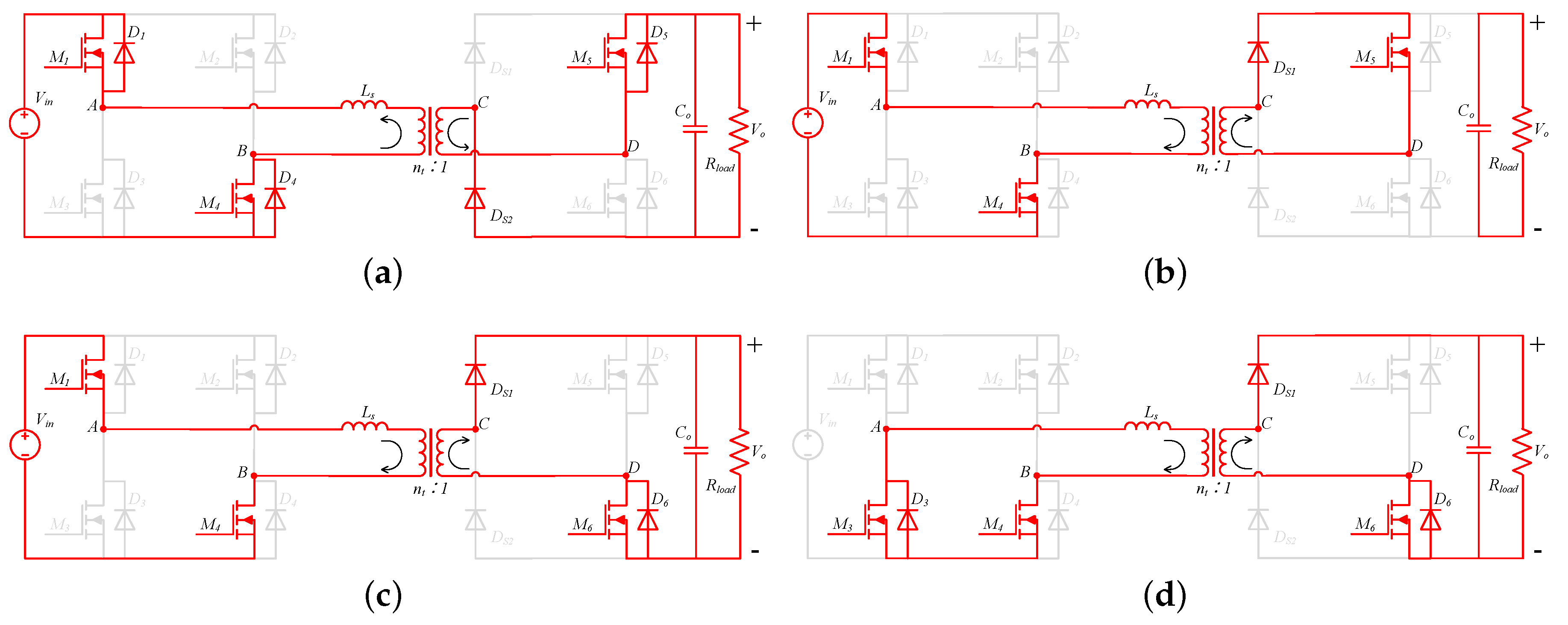
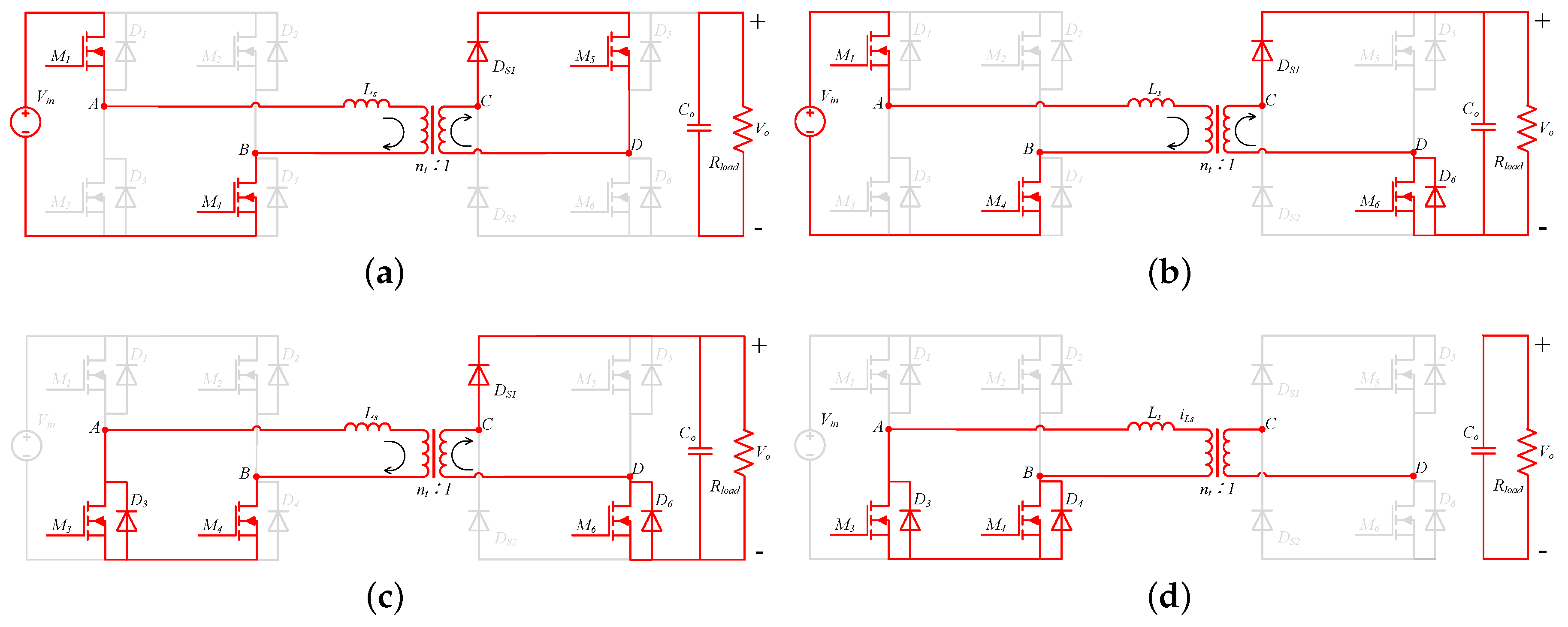
The ideal steady-state waveforms in Mode A are shown in Figure 2, where denotes the first zero-crossing points referred to the turn-on moment of . It can be seen that Mode A is featured with ; and there are eight different intervals in one switching period. The corresponding equivalent circuits of the first four intervals are presented in Figure 3, respectively. The other four intervals are almost the same except for the directions of voltage/current and involved conducting devices.
Interval 1 [Figure 3a]: At the beginning, is turned off and is turned on with ZVS. In this interval, the conducting devices are and , and . Thus, the voltage across the inductor is clamped at , the value of decreases linearly from the negative value to . The power stored in the inductor is delivered to input DC power and load during this interval:
Interval 2 [Figure 3b]: At , the polarity of is changed, the current flowing diode-leg is shifted naturally from to , i.e., is turned off with zero current. The secondary-side of transformer is shorted now by and . Meanwhile, the primary current flows from to through primary switches and . Thus, the voltage across the inductor is clamped at , the value of increases linearly from to the positive maximum . The power is being stored in the inductor during this interval:
Interval 3 [Figure 3c]: At (), is turned off and is turned on with ZVS. In this interval, the situation on the primary side does not change; the secondary current is shifted to and , flowing to the load. Thus, during this interval, the voltage across inductor is clamped at , and the power is transmitted to the load. Due to , the value of starts to decrease linearly from to the positive value :
Interval 4 [Figure 3d]: At , is turned off and is turned on with ZVS. In this interval, the primary side is shorted by and ; and no change happens on the secondary side. Thus, the voltage across inductor is clamped at . During this interval, the value of starts to decrease linearly until it reaches . The power stored in the inductor is delivered to load:
Based on Equations (1)–(4), the instantaneous current values at the moments of transition can be calculated as functions of and . Furthermore, the output power and the inductor RMS current can be obtained too. These results are listed in Table 1, where the current and power values are normalized by the following base values:
2.3. Steady-State Analysis of Discontinuous-Current Mode
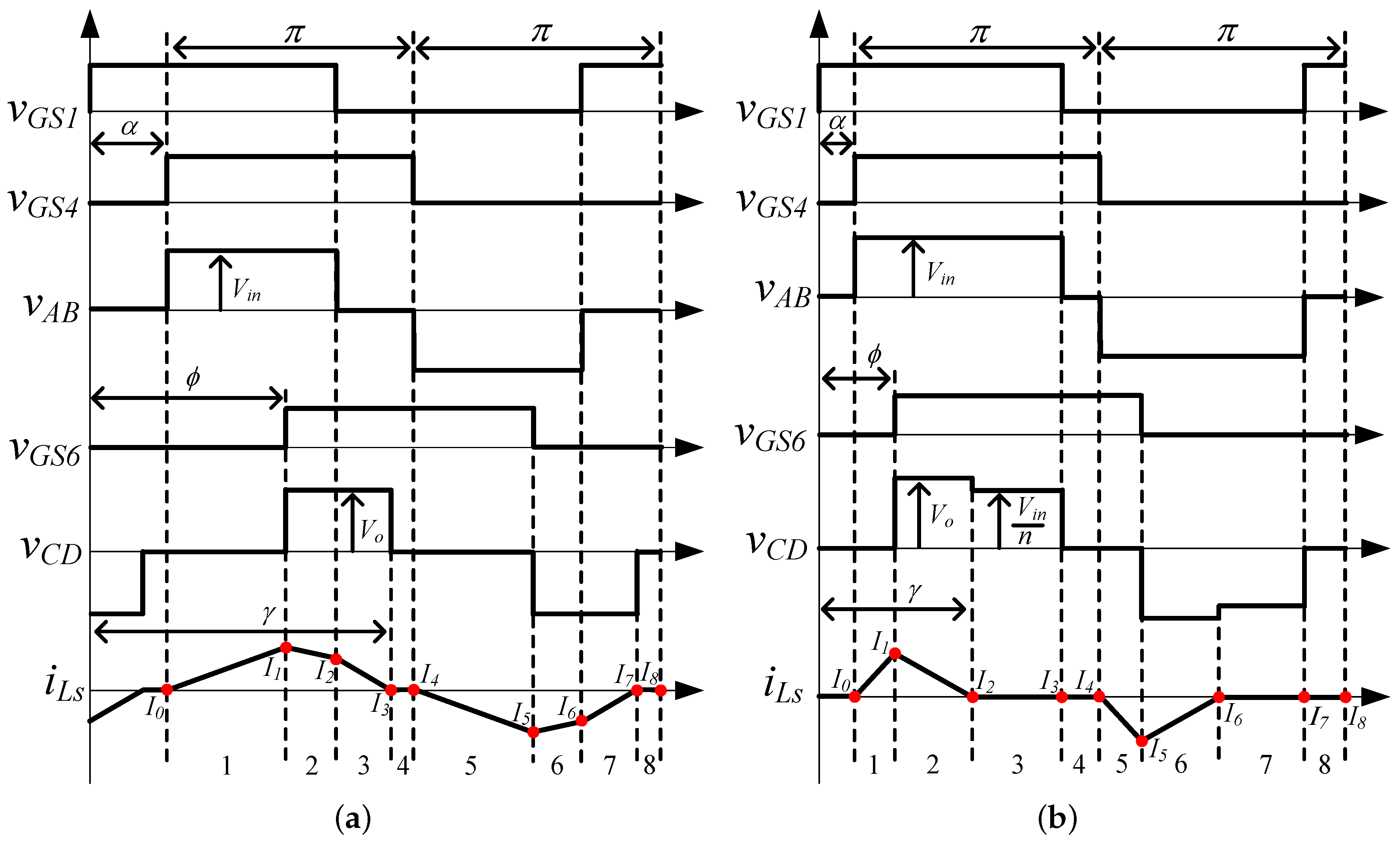
Different from CCM, the inductor current in DCM remains at zero for a small duration in each switching period. Steady-state waveforms of two DCMs are shown in Figure 4, where denotes the second zero-crossing points referring to the turn-on moment of . It can be found that the difference between those two DCMs can be concluded as: for Mode B and for Mode C.
Mode B [Figure 4a]
According to the steady-state waveforms in Mode B, the equivalent circuits in the first four intervals are shown in Figure 5. It can be seen that the first three intervals in Mode B are almost the same as Intervals 2–4 in Mode A, except that the inductor current at the end of Interval 3 (Mode B) can arrive again at zero.
Interval 4 [Figure 5d]: After , all secondary diodes are reversed biased, which will result in the secondary-side of transformer being open-circuited. Meanwhile, the primary switches and are still conducting. Thus, the transformer secondary voltage is clamped at 0, and is kept at zero. This interval ends up with turned on at zero current. In this zero-current interval, there is no power transferring in the converter.
Mode C [Figure 4b]
Similarly, the equivalent circuits corresponding to first four intervals in Mode C are shown in Figure 6, respectively. It can be seen that the first second intervals in Mode C are almost the same as Intervals 2 and 3 in Mode A, except that the inductor current at end of Interval 2 (Mode C) can arrive again at zero.
Interval 3 [Figure 6c] in Mode C is different from those aforementioned intervals. Although the input DC source is applied on the primary-side of transformer by the switches and , there is no flowing current in the converter. The secondary-side of transformer is open-circuited since all secondary diodes are reversed biased. Thus, the secondary-side transformer voltage is clamped at . Interval 3 ends up with turned on at zero current. This interval also belongs to the zero-current interval, and there is no power transferring. Interval 4 is the same as Interval 4 in Mode B.
Based on the steady-state analysis in each DCM, the instantaneous current values at the moment of transition can be calculated. Similarly, the output power and RMS current across inductor can be also obtained. These theoretical results are listed in Table 2.
2.4. Switching Behaviour
Since the converter may work in three different steady-state modes, the switching behaviour of all switches and diodes also vary with the operation modes. According to the current polarity at switching moment of all switches and diodes, the switching behaviour in each mode are concluded in Table 3. First of all, the diodes in the secondary H-bridge can be turned on/off at zero current in any mode. In Mode A, all switches operate with ZVS and each diode is turned on/off with zero-current. Compared with Mode A, the switching loss in two DCMs is slightly increased due to the partial switch losing ZVS, and the switching loss in Mode C is higher than those in Mode B. Thus, Mode A should be selected as the main operation mode.
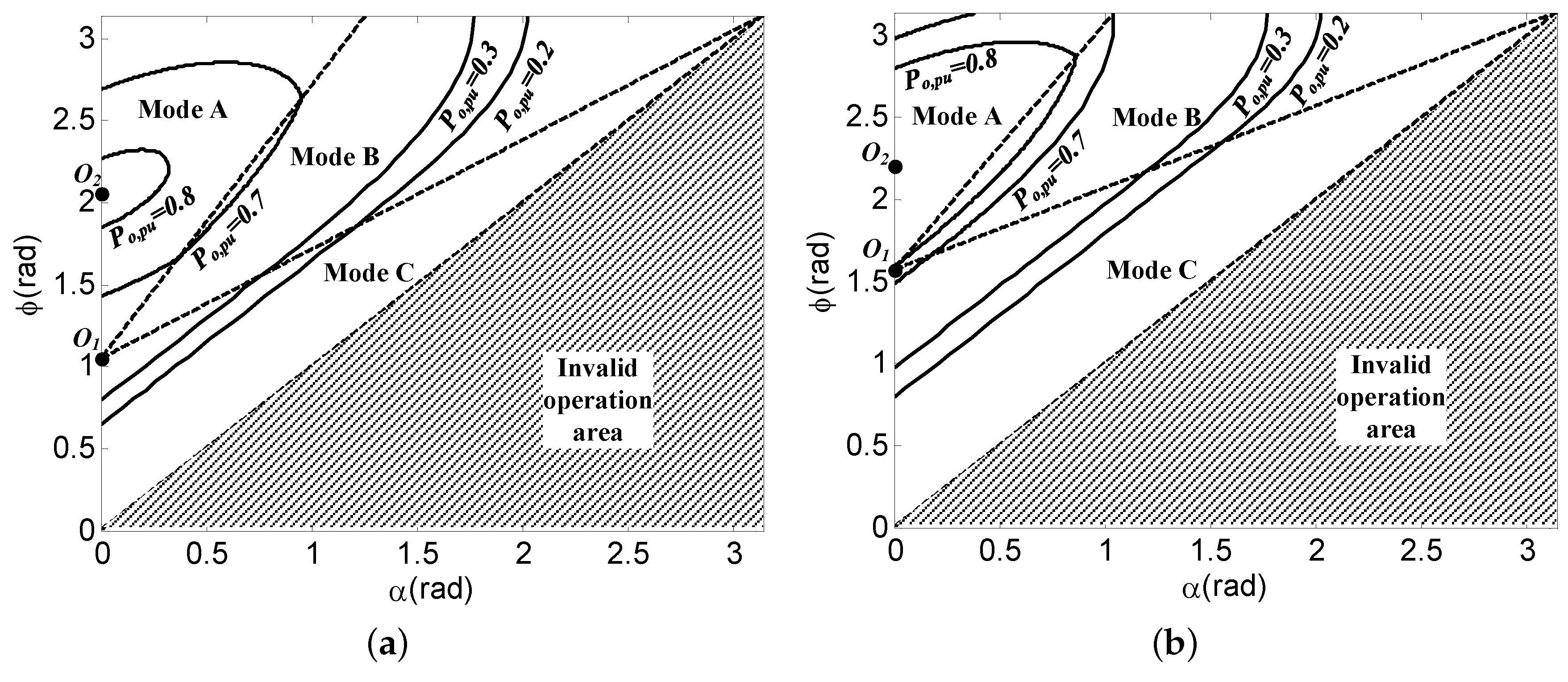
2.5. Operation Range of Each Mode
Through comparing three steady-state modes, it can be found that Mode B is an in-between mode, and there are two boundary conditions existing between Mode B and the other two modes. Thus, the operating range of two controllable phase-shifts and will be different in each mode. Knowing these conditions and range is helpful for the design of the converter.
When in Mode B, the converter works at the boundary condition (6) between Mode A and B. At this boundary, the secondary H-bridge works in synchronous rectification mode:
When in Mode B, it works at another boundary condition (7) between those two DCMs, in which the second zero-crossing happens at the moment of the switch being turned on:
According to both boundary conditions, the operating range of each mode is shown in Figure 7 for and , respectively.
In Figure 7, the shaded area represents an invalid operation area. The boundary of the neighboring modes is plotted by two dashed lines using (6) and (7), respectively, and these two boundary lines intersect at the point . Meanwhile, the power contours with the same normalized power value are shown by solid curves, in which the maximum load capacity of the converter is located at the point , . The operating range with the conventional secondary phase-shifted control is only along the -axis. Compared with conventional control, PPWM + SPS can expand regulating range of output power and enhance flexibility of phase-shift control.
3. Proposed Control Route of an S-DAB Converter with PPWM + SPS Control
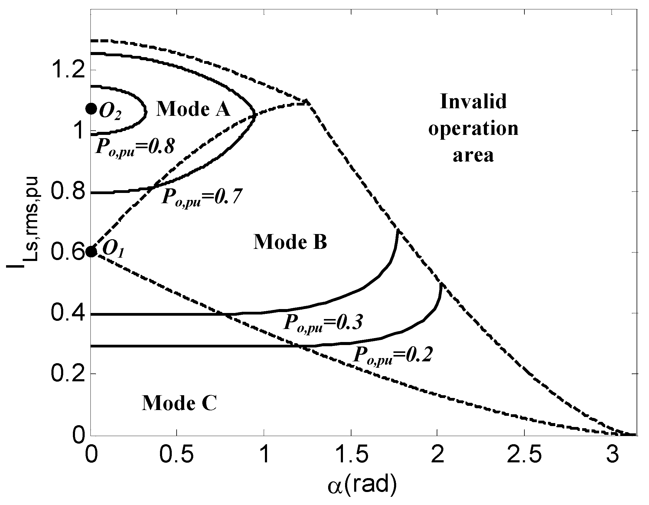
It is obvious that countless control routes exist from full power at to zero power at for an S-DAB converter with PPWM + SPS control in Figure 7. Therefore, in order to select a reasonable control route, theoretical analysis of the inductor current is carried out to achieve lower conducting loss.
Based on Table 1 and Table 2, the relationship between normalized inductor RMS current and phase-shift at different power contours are shown in Figure 8, with as an example. It can be found that, at the high power levels, the converter may work in Mode A. values can arrive at the minimum values when the converter is operated at conventional secondary phase-shifted control from to along the -axis. At the low power levels from to zero power , the converter may operate in Mode C, in which is minimum and constant for the same power level.
In practical application, each switch and diode has its own snubber/parasitic capacitor. It is possible to get the voltage ringing on the transformer secondary-side when the converter is working in a zero-current interval. In Mode C, there are two zero-current Intervals (3 and 4) in the half period. Taking a capacitor into account, Interval 3 can be equivalent to the new circuit as Figure 9. In this interval, a resonance circuit is formed by a power inductor and the snubber/parasitic capacitor of the diode leg. Thus, the voltage ringing will be introduced into the transformer secondary-side. However, there is no voltage ringing in Interval 4. The main reason is that the DC source in Figure 9 is short-circuited in interval 4. Compared with Mode C, there is only one zero-current interval in Mode B and it is free of voltage ringing, which is same as Interval 4 in Mode C. Considering that voltage ringing will potentially bring up system instability and damage the semiconductor devices, the control route for low power is put on the boundary line between Mode B and C. Thus, the selected route from full power to zero power with PPWM + SPS control is given as Equations (8) and (9), which is a piecewise function. Under the proposed route control, the converter can achieve at the minimum RMS current for the full power range and is free of voltage ringing across the transformer.
When ,
When ,
where , .
4. Experimental Verifications
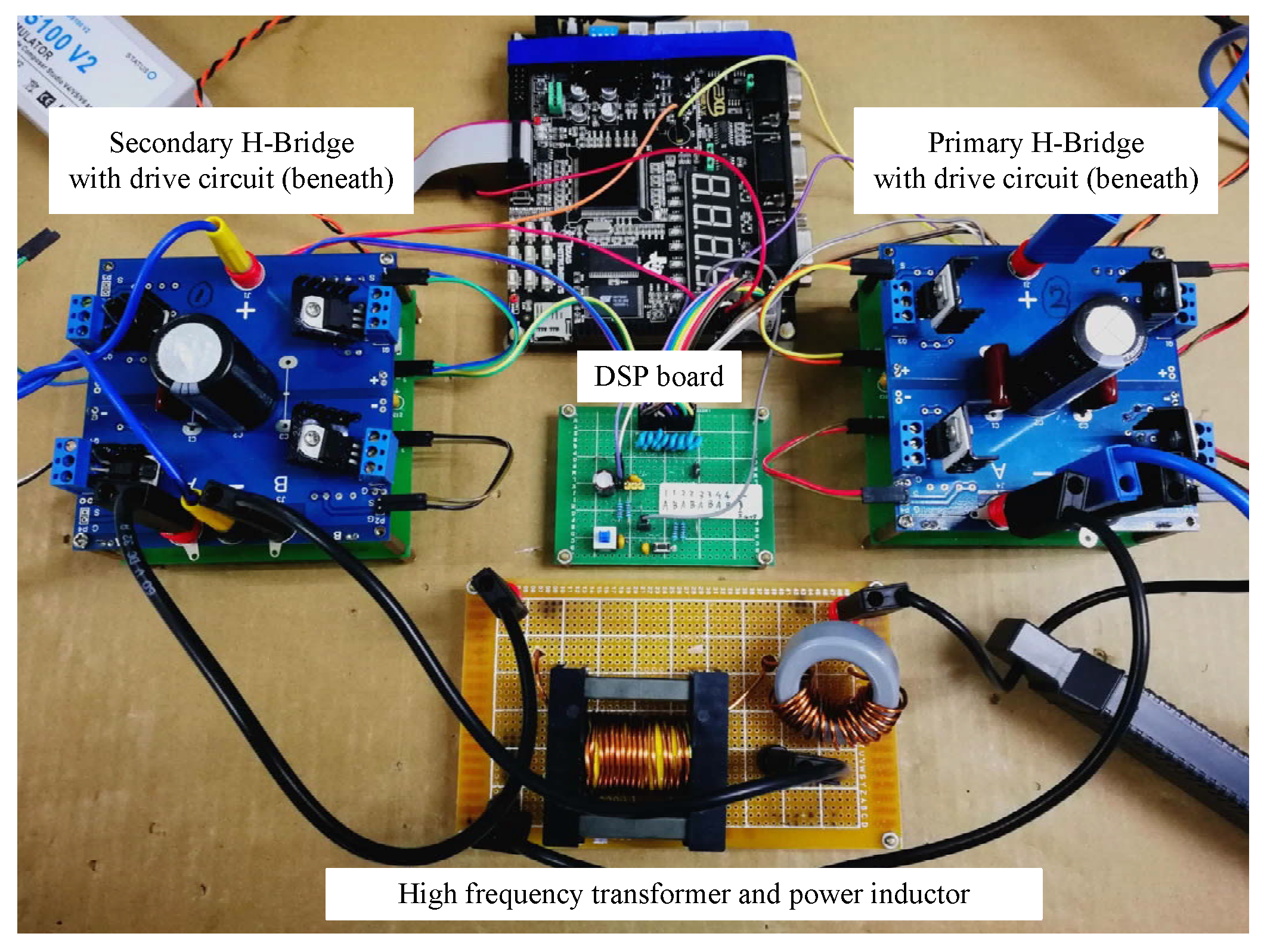
To verify the theoretical analysis above, a 200 W S-DAB prototype is built, as shown in Figure 10. The specifications of the lab-scale converter are listed in Table 4. The gating signals of S-DAB are implemented using a TMS320F28335 DSP from TI (Texas Instruments, Dallas, TX, USA) and the switching frequency is set at 100 kHz.
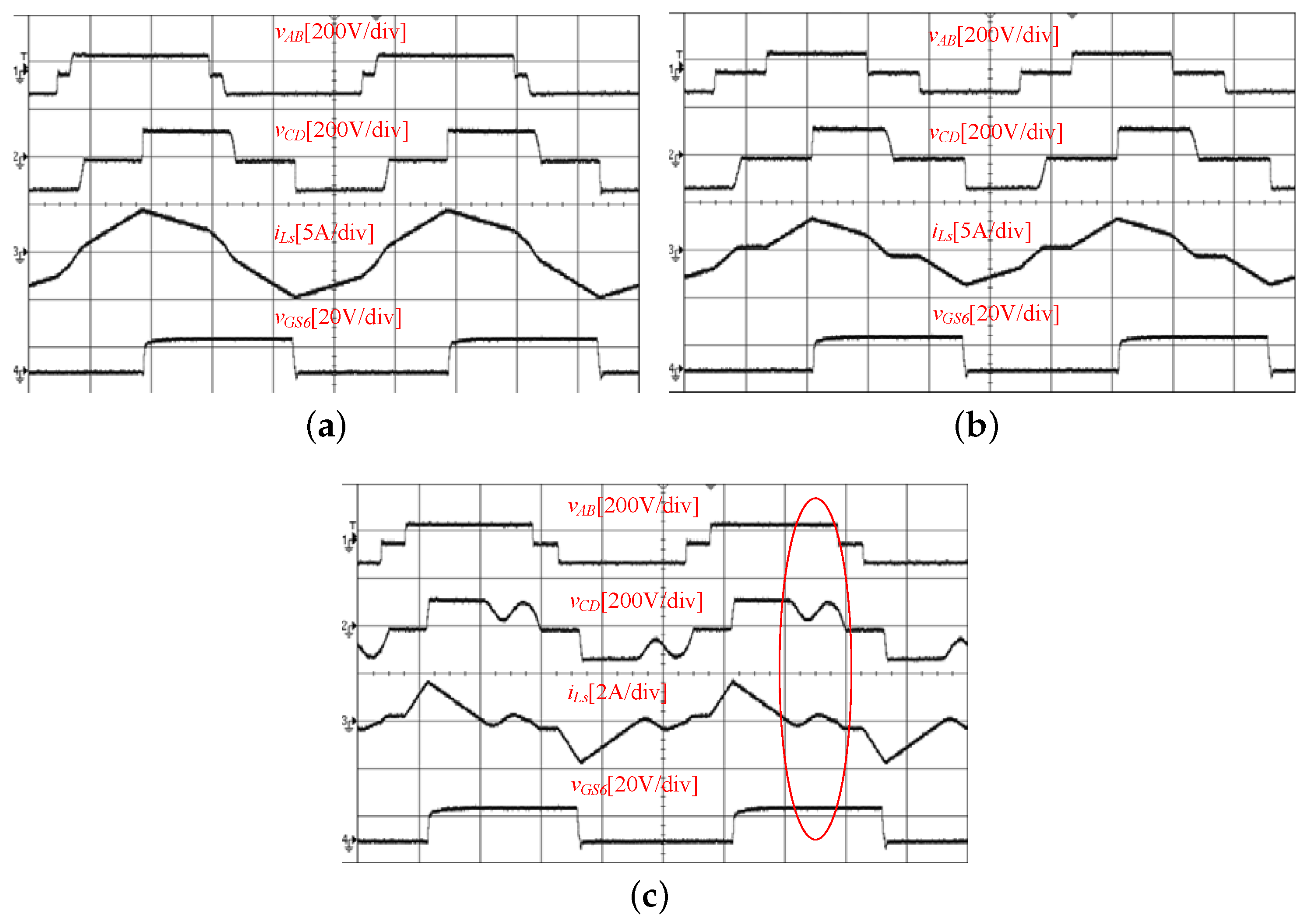
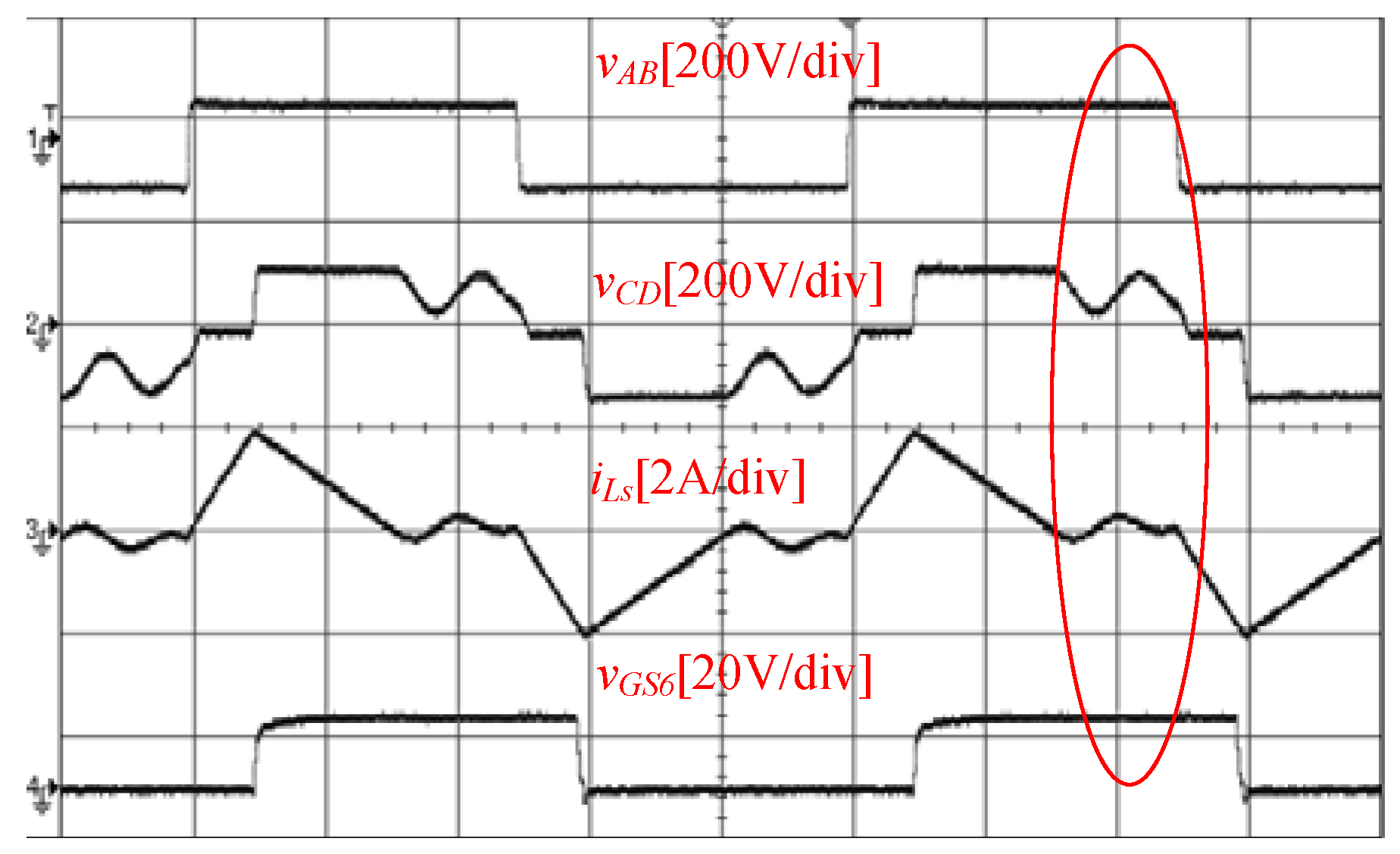
Based on the analysis of each operation mode in Section 2, a set of experimental waveforms corresponding to three effective modes are obtained and shown in Figure 11, respectively. These experimental results match the theoretical prediction closely. In Figure 11c, the voltage ringing shows up on the transformer secondary-side after decreases to zero and remains a small duration until . As expected, the voltage ringing is not identified in Figure 11b.
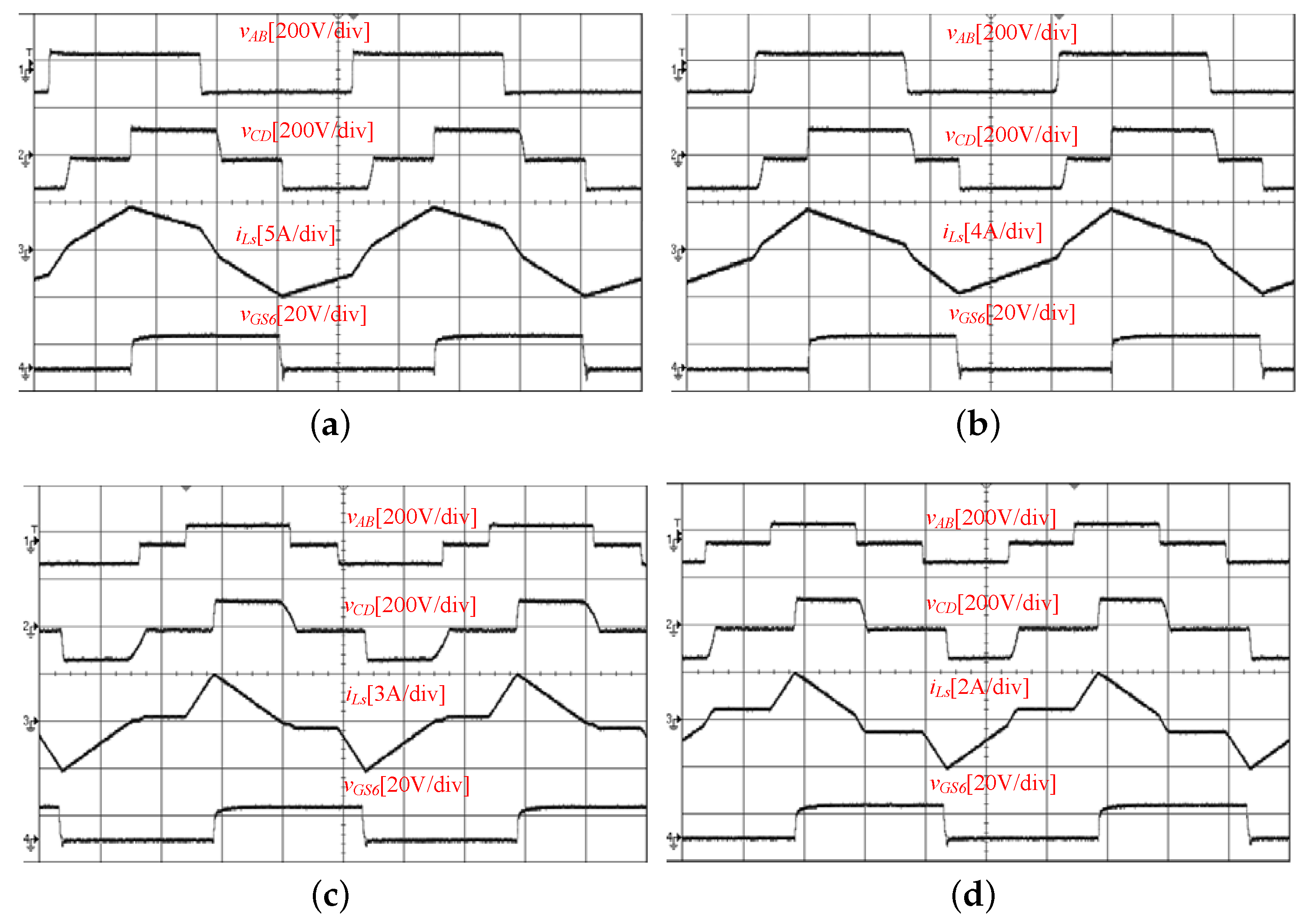
A series of experimental tests are then performed along the proposed minimized rms current route. The boundary power between the two stages of the control route is calculated to be 52% load, i.e., 104 W. Thus, the converter works in CCM (Mode A) at the high power of 200 W and 150 W. Two phase-shift angles are calculated as , (200 W) and , (150 W) according to (8). Experimental results of 200 W and 150 W are shown in Figure 12a,b, respectively. It can be seen from those two figures that the inductor current is continuous. The related waveforms satisfy the operation condition of and all switches can operate at ZVS.
When the output power is lower than 52% load, the converter is operated at the boundary between Mode B and C. Using (9), two phase-shift angles are obtained as follows: (1) 100 W, , ; (2) 50 W, , . Experimental results of 100 W and 50 W are shown in Figure 12c,d, respectively. It can be seen that the transition moment of from to zero happens at the zero-crossing point of the inductor current and there is a small zero-current duration. The operation conditions of two experimental results match the boundary feature between both DCMs. In addition, the voltage ringing on the waveform is prevented in comparison to DCM under conventional secondary phase-shifted control (Figure 13). Based on these experimental results, the values of the RMS current, peak current, and efficiency are listed in Table 5, where the highest efficiency can arrive at 95.53% for 150 W. For 50 W operation with conventional control in Figure 13, the measured efficiency is 88.46%. It is seen that the efficiency using the proposed control is improved slightly since the current values and the switching behaviour under the two control methods are almost the same and the loss due to the ringing accounts for a small portion of total loss. However, the removal of the ringing phenomenon depresses EMI so that the risk of distortion in gating signals is reduced and the operation stability is improved consequently.
5. Conclusions
In this work, PPWM + SPS control with two controllable phase-shifts is applied on an S-DAB converter for boost operation and all effective steady-state modes are identified. Based on the characteristics of each mode, a reasonable control route is developed and implemented on a lab-scale S-DAB prototype. The experimental results show the consistency with the theoretical analysis results. Compared with conventional secondary phase-shifted control, the proposed control route not only makes the converter operate with the minimized RMS current for the whole power range, but also eliminates the voltage ringing on the secondary-side of the HF transformer completely. More importantly, the proposed hybrid control can be also applied on the other S-DAB converters in [22,23,24] to prevent the voltage ringing and improve stability. In addition, other optimization objectives could be developed according to various application requirements.
Author Contributions
M.L. did theoretical analysis, derivation, circuit implementation, experimental test and paper writing. X.L. was responsible for planning, coordination and proofreading.
Funding
This research was funded by Fundo para o Desenvolvimento das Ciências e da Tecnologia under Grant No. 004/2015/A1.
Acknowledgments
The authors would like to acknowledge Song Hu, Guo Chen for their support in the preparation of circuit implementation.
Conflicts of Interest
The authors declare no conflict of interest.
References
- Blaabjerg, F.; Chen, Z.; Kjaer, S.B. Power electronics as efficient interface in dispersed power generation systems. IEEE Trans. Power Electron. 2004, 19, 1184–1194. [Google Scholar] [CrossRef]
- Tahir, S.; Wang, J.; Baloch, M.; Kaloi, G. Digital control techniques based on voltage source inverters in renewable energy applications: A review. Electronics 2018, 7, 18. [Google Scholar] [CrossRef]
- Chen, Z.; Guerrero, J.M.; Blaabjerg, F. A review of the state of the art of power electronics for wind turbines. IEEE Trans. Power Electron. 2009, 24, 1859–1875. [Google Scholar] [CrossRef]
- Abdelsalam, A.K.; Massoud, A.M.; Ahmed, S.; Enjeti, P.N. High-performance adaptive perturb and observe MPPT technique for photovoltaic-based microgrids. IEEE Trans. Power Electron. 2011, 26, 1010–1021. [Google Scholar] [CrossRef]
- Almalaq, Y.; Matin, M. Three topologies of a non-isolated high gain switched-inductor switched-capacitor step-up cuk converter for renewable energy applications. Electronics 2018, 7, 94. [Google Scholar] [CrossRef]
- Lee, W.J.; Kim, C.E.; Moon, G.W.; Han, S.K. A new phase-shifted full-bridge converter with voltage-doubler-type rectifier for high-efficiency PDP sustaining power module. IEEE Trans. Ind. Electron. 2008, 55, 2450–2458. [Google Scholar]
- Cha, H.; Chen, L.; Ding, R.; Tang, Q.; Fang, Z.P. An alternative energy recovery clamp circuit for full-bridge PWM converters with wide ranges of input voltage. IEEE Trans. Power Electron. 2008, 23, 2828–2837. [Google Scholar]
- Chen, W.; Ruan, X.; Zhang, R. A novel zero-voltage-switching PWM full bridge converter. IEEE Trans. Power Electron. 2008, 23, 793–801. [Google Scholar] [CrossRef]
- Jang, Y.; Jovanovic, M.M.; Chang, Y.-M. A new ZVS-PWM full-bridge converter. IEEE Trans. Power Electron. 2003, 18, 1122–1129. [Google Scholar] [CrossRef]
- Yoon, H.K.; Han, S.K.; Choi, E.-S.; Moon, G.-W.; Youn, M.-J. Zero-voltage switching and soft-commutating two-transformer full-bridge PWM converter using the voltage-ripple. IEEE Trans. Ind. Electron. 2008, 55, 1478–1488. [Google Scholar] [CrossRef]
- Lee, I.O.; Moon, G.W. Phase-shifted PWM converter with a wide ZVS range and reduced circulating current. IEEE Trans. Power Electron. 2013, 28, 908–919. [Google Scholar] [CrossRef]
- Jang, Y.; Jovanovic, M.M. A new family of full-bridge ZVS converters. IEEE Trans. Power Electron. 2004, 19, 701–708. [Google Scholar] [CrossRef]
- Ruan, X.; Yan, Y. A novel zero-voltage and zero-current-switching PWM full-bridge converter using two diodes in series with the lagging leg. IEEE Trans. Ind. Electron. 2001, 48, 777–785. [Google Scholar] [CrossRef]
- Lo, Y.K.; Lin, C.Y.; Hsieh, M.T.; Lin, C.Y. Phase-shifted full-bridge series-resonant DC-DC converters for wide load variations. IEEE Trans. Ind. Electron. 2011, 58, 2572–2575. [Google Scholar] [CrossRef]
- Gautam, D.S.; Bhat, A.K.S. A comparison of soft-switched DC-to-DC converters for electrolyzer application. IEEE Trans. Power Electron. 2013, 28, 54–63. [Google Scholar] [CrossRef]
- Ali, K.; Das, P.; Panda, S.K. Analysis and design of APWM half-bridge series resonant converter with magnetizing current assisted ZVS. IEEE Trans. Ind. Electron. 2017, 64, 1993–2003. [Google Scholar] [CrossRef]
- Mumtahina, U.; Wolfs, P.J. Multimode optimization of the phase shifted LLC eries resonant converter. IEEE Trans. Power Electron. 2018, 1. [Google Scholar] [CrossRef]
- Lee, I.O.; Moon, G.W. The k-Q Analysis for an LLC series resonant converter. IEEE Trans. Power Electron. 2014, 29, 13–16. [Google Scholar] [CrossRef]
- Fang, X.; Hu, H.; Chen, F.; Somani, U.; Auadisian, E.; Shen, J.; Batarseh, I. Efficiency-oriented optimal design of the LLC resonant converter based on peak gain placement. IEEE Trans. Power Electron. 2013, 28, 2285–2296. [Google Scholar] [CrossRef]
- Zhang, J.; Zhang, F.; Xie, X.; Jiao, D.; Qian, Z. A novel ZVS DC/DC converter for high power applications. IEEE Trans. Power Electron. 2004, 19, 420–429. [Google Scholar] [CrossRef]
- Mishima, T.; Nakaoka, M. Practical evaluations of a ZVS-PWM DC-DC converter with secondary-side phase-shifting active rectifier. IEEE Trans. Power Electron. 2011, 26, 3896–3907. [Google Scholar] [CrossRef]
- Kulasekaran, S.; Ayyanar, R. Analysis, design, and experimental results of the semidual-active-bridge converter. IEEE Trans. Power Electron. 2014, 29, 5136–5147. [Google Scholar] [CrossRef]
- Li, W.; Zong, S.; Liu, F.; Yang, H.; He, X.; Wu, B. Secondary-side phase-shift-controlled ZVS DC/DC converter with wide voltage gain for high input voltage applications. IEEE Trans. Power Electron. 2013, 28, 5128–5139. [Google Scholar] [CrossRef]
- Wu, H.; Chen, L.; Xing, Y. Secondary-side phase-shift-controlled dual-transformer-based asymmetrical dual-bridge converter with wide voltage gain. IEEE Trans. Power Electron. 2015, 30, 5381–5392. [Google Scholar] [CrossRef]
- Hu, S.; Li, X. Performance evaluation of a semi-dual-bridge resonant DC/DC converter with secondary phase-shifted control. IEEE Trans. Power Electron. 2017, 32, 7727–7738. [Google Scholar] [CrossRef]
- Hu, S.; Li, X.; Lu, M.; Luan, B.-Y. Operation modes of a secondary-side phase-shifted resonant converter. Energies 2015, 8, 12314–12330. [Google Scholar] [CrossRef]
- Park, K.B.; Kim, C.E.; Moon, G.W.; Youn, M.J. Voltage oscillation reduction technique for phase-shift full-bridge converter. IEEE Trans. Ind. Electron. 2007, 54, 2779–2790. [Google Scholar] [CrossRef]
- Garabandic, D.; Dunford, W.G.; Edmunds, M. Zero-voltage-zero-current switching in high-output-voltage full-bridge PWM converters using the interwinding capacitance. IEEE Trans. Power Electron. 1999, 14, 343–349. [Google Scholar] [CrossRef]
Figure 1.
The circuit configuration of a S-DAB converter.

Figure 2.
Steady-state waveforms in Mode A.

Figure 3.
Equivalent circuits corresponding to the first four intervals in Mode A: (a) Interval 1 []; (b) Interval 2 []; (c) Interval 3 []; (d) Interval 4 [].
Figure 3.
Equivalent circuits corresponding to the first four intervals in Mode A: (a) Interval 1 []; (b) Interval 2 []; (c) Interval 3 []; (d) Interval 4 [].

Figure 4.
Steady-state waveforms in: (a) Mode B; (b) Mode C.

Figure 5.
Equivalent circuits corresponding to the first four intervals in Mode B: (a) Interval 1 []; (b) Interval 2 []; (c) Interval 3 []; (d) Interval 4 [].
Figure 5.
Equivalent circuits corresponding to the first four intervals in Mode B: (a) Interval 1 []; (b) Interval 2 []; (c) Interval 3 []; (d) Interval 4 [].

Figure 6.
Equivalent circuits corresponding to the first four intervals in Mode C: (a) Interval 1 []; (b) Interval 2 []; (c) Interval 3 []; (d) Interval 4 [].
Figure 6.
Equivalent circuits corresponding to the first four intervals in Mode C: (a) Interval 1 []; (b) Interval 2 []; (c) Interval 3 []; (d) Interval 4 [].

Figure 7.
Operating range of each boost mode with suspended power contours for and : (a) ; (b) .

Figure 8.
Normalized inductor RMS current vs. phase-shift at different power contours for .

Figure 9.
New equivalent circuit corresponding to interval 3 in Mode C.

Figure 10.
The layout of a W S-DAB laboratory prototype.

Figure 11.
Experimental waveforms of , , and (from top–bottom), time scale: (2 s/div), (a) Mode A; (b) Mode B; (c) Mode C.
Figure 11.
Experimental waveforms of , , and (from top–bottom), time scale: (2 s/div), (a) Mode A; (b) Mode B; (c) Mode C.

Figure 12.
Experimental waveforms at four different power levels under the proposed route for V and V, time scale: (2 s/div), (a) 200 W; (b) 150 W; (c) 100 W; (d) 50 W.
Figure 12.
Experimental waveforms at four different power levels under the proposed route for V and V, time scale: (2 s/div), (a) 200 W; (b) 150 W; (c) 100 W; (d) 50 W.

Figure 13.
Experimental waveforms at 50 W with conventional secondary phase-shifted control.


Table 1.
Theoretical values of inductor current and output power in Mode A.
| Value | Expression |
|---|---|
| 0 | |
Table 2.
Theoretical values of inductor current and output power in DCM.
| Value | Mode B | Mode C |
|---|---|---|
| 0 | 0 | |
| 0 | ||
| 0 | 0 | |
Table 3.
Switching behavior in different modes.
| Mode | , | , | , | , |
|---|---|---|---|---|
| A | ZVS | ZVS | ZVS | zero-current-on/off |
| B | ZVS | zero-current-on/off | ZVS | zero-current-on/off |
| C | zero-current-on/off | zero-current-on/off | ZVS | zero-current-on/off |
Table 4.
Specifications of a 200 W S-DAB converter.
| Component | Parameter |
|---|---|
| Input DC voltage | 80 V |
| Load DC voltage | 120 V |
| Power inductance | 38 H, CM400125/MPPcore |
| Transformer turns ratio | 15:15, ETD49/N97 |
| Filter capacitor | 470 F, 1 electrolytic cap |
| Switch ∼ | STP40NF20, m |
| Diode , | MBR40250TG, V |
Table 5.
Measured results at V and V.
| Power | (A) | (A) | (%) | |
|---|---|---|---|---|
| 200 W | theor. | 2.9 | 4.52 | - |
| exp. | 3.08 | 4.7 | 94.97% | |
| 150 W | theor. | 2.14 | 3.63 | - |
| exp. | 2.19 | 3.63 | 95.53% | |
| 100 W | theor. | 1.57 | 2.96 | - |
| exp. | 1.58 | 2.92 | 92.13% | |
| 50 W | theor. | 0.94 | 2.1 | - |
| exp. | 0.95 | 2.07 | 88.95% | |
© 2018 by the authors. Licensee MDPI, Basel, Switzerland. This article is an open access article distributed under the terms and conditions of the Creative Commons Attribution (CC BY) license (http://creativecommons.org/licenses/by/4.0/).
Share and Cite
MDPI and ACS Style
Lu, M.; Li, X. Performance Evaluation of a Semi-Dual-Active-Bridge with PPWM Plus SPS Control. Electronics 2018, 7, 184. https://doi.org/10.3390/electronics7090184
AMA Style
Lu M, Li X. Performance Evaluation of a Semi-Dual-Active-Bridge with PPWM Plus SPS Control. Electronics. 2018; 7(9):184. https://doi.org/10.3390/electronics7090184
Chicago/Turabian StyleLu, Ming, and Xiaodong Li. 2018. "Performance Evaluation of a Semi-Dual-Active-Bridge with PPWM Plus SPS Control" Electronics 7, no. 9: 184. https://doi.org/10.3390/electronics7090184
Note that from the first issue of 2016, this journal uses article numbers instead of page numbers. See further details here.