Research on an Auto-Optimized Capacitor Voltage Balancing Control Strategy of MMC SM for Renewable Energy HVDC Transmission System


1
School of Mechatronic Engineering and Automation, Shanghai University, Baoshan District, Shanghai 200444, China
2
Department of Electrical Engineering, Tongji University, Yangpu District, Shanghai 200092, China
*
Author to whom correspondence should be addressed.
Electronics 2019, 8(1), 104; https://doi.org/10.3390/electronics8010104
Submission received: 11 December 2018
/
Revised: 6 January 2019
/
Accepted: 14 January 2019
/
Published: 18 January 2019
(This article belongs to the Special Issue Renewable Electric Energy Systems)
Abstract
:The Modular Multilevel Converter (MMC) is one of the most attractive converter topologies in the High Voltage Direct Current (HVDC) transmission field. The latest widely used sorting method has a low algorithm complexity. It can effectively balance the sub-module (SM) capacitor voltages, but it would cause relatively high switching frequency and power loss. Aiming at the problem that the sub-module (SM) capacitor voltage sorting algorithm has a large switching loss due to the high switching frequency of the device, this paper proposes an auto-optimized capacitor voltage balancing control strategy. Firstly, the topology and operation principle of MMC are analyzed. Secondly, a SM capacitor voltage control method based on the dynamic deviation threshold is proposed. Considering the switch switching state of the SM and the difference between the voltages of each SM, the algorithm can obtain the dynamic deviation valve using the closed-loop control. The method can avoid the unnecessary repeated switching of the Insulated Gate Bipolar Transistor (IGBT) under the premise of ensuring that the capacitance voltages of the SMs are basically the same, which effectively result in reducing the switching frequency of the MMC SM and reducing the switching loss, thereby improving the operating efficiency of the system. Finally aiming at the proposed control strategy, the simulation and experimental verification are carried out which shows that the proposed algorithm can better control the system voltage deviation, reduce the switching loss of the system and improve the stability of the system.
1. Introduction
The modular multilevel converter (MMC), first proposed by Marquardt and Lesnicar in 2003 [1], has become the most attractive topology for high voltage applications. Over the past decade, extensive research has been focused on the technical challenges associated with the designs, operation and control of the MMC to improve its performance for various applications [2,3,4,5,6,7,8,9,10,11,12,13]: voltage source converter-based high voltage direct current transmission (VSC-HVDC) [5,6,7,8]. Authors of References [9,10,11] give the independent active and reactive power control strategies of MMC from single system to a dual system in detail. MMC is also used in high voltage variable speed drives [12,13], etc. The MMC topology consists of a number of identical sub-modules (SMs), each consisting of a semiconductor switching device with a lower rated voltage. When the MMC is in the inverter state, the number of SMs determines the number of levels on the alternating current (AC) output side. It has many advantages over other multilevel inverters such as diode clamp multilevel, flying capacitors and cascaded H bridges. According to References [14,15,16,17], it can be summarized as follows:
- High efficiency: since the required switching frequency is low and the switching loss is small, the MMC is characterized by high efficiency operations.
- Scalability and modularity: MMC has the flexibility to easily increase the rated voltage by cascading more SMs. At the same time, when a SM fails, it can be bypassed, is easy to replace the faulty SM without power failure, and has high redundancy.
- Better harmonic performance: the number of MMC SMs is generally several tens or more, so the output level of MMC is more than other topologies. Since the number of levels on the output side is larger, the filtered waveform is closer to sinusoidal and the harmonic content is relatively less, so it has a low harmonic distortion, allowing the use of smaller filter characteristics.
Due to the above advantages, MMC provides a suitable and flexible converter topology that can be adapted to different ranges of voltages and powers. However, one of the potential challenges of MMC is the SM capacitor voltage balancing. In practice, capacitor voltage imbalance is a serious threat to the reliable operation of MMC systems [18]. In order to guarantee the stable operation of MMC at various operating points (e.g., currents and voltages), it is important to evenly distribute the voltage of multiple floating capacitors among each SM. Many capacitor voltage balancing approaches have been proposed in the literature [18,19,20,21,22,23,24]. The simplest way to balance the capacitor voltage is through the periodic rotation [15] of the gated mode based on the phase voltage switching state redundancy. However, control for an MMC with a large number of SM is very complicated.
The literature [19,20,21] uses different methods to reduce the capacitance voltage deviation between SMs. In References [20], the SM capacitor voltage is balanced by a carrier-based pulse width modulation method. This method can better reduce the capacitance voltage deviation between SMs, but it is necessary to add a controller to each SM for control, which increases economic cost and system complexity. In Reference [20], the capacitance voltage deviation between SMs is reduced by adjusting the duration of the PWM pulses. However, as the number of SMs per arm increases, the computational complexity of the method increases. The algorithm based on a sorting technique is given in Reference [21]. In this method, the computational complexity is reduced and the capacitance voltage deviation between SMs is well suppressed compared to the previous methods, but the switching frequency of the system is high. The equalization algorithm proposed above is applicable to a high-power and high-voltage MMC system and can better reduce the capacitance voltage deviation between SMs, but the system has a large open loss.
In References [22,23,24,25,26], if the SM capacitor voltage deviation is within the acceptable range of the system, the SM switching frequency is reduced by different methods. In References [22,23], the SM operating state is determined according to the direction of the bridge arm current and change trend of the reference voltage. In Reference [24], a method of fixing the switching frequency is proposed. By using a fixed module rotation number in each control cycle, the frequent switching issue of the SMs is avoided. However, a fixed module rotation number can only be obtained by multiple simulation tests. Reference [25] proposed a coefficient of variation (CV) algorithm, which can reduce the switching frequency by setting CV, but the value of CV is not easy to choose. Hofmann, V., et.al. [26] proposed a balance control algorithm (BCA), which adjusts the switching frequency, but the balance effect is not ideal. The algorithm proposed above can better reduce the open loss of the system, but the capacitance voltage deviation between SMs cannot be well suppressed.
It can be seen from the literature analysis that the proposed balancing algorithm could not solve the switching frequency and capacitance voltage deviation of the SM simultaneously. Therefore, based on the analysis of the working principles of MMC topology and sorting algorithm, an auto-optimized capacitor voltage balancing method based on a maximum voltage deviation automatic threshold for a modular multilevel converter is proposed in this paper, which can reduce the switching frequency of the system and the deviation of the capacitor voltage.
The outline of this paper is as follows. In Section 2, the topology and operating principles of the MMC and a detailed analysis of the proposed auto-optimized capacitor voltage balancing method are presented. In Section 3, a 21-level and a 5-level MMC simulation model are used to verify the proposed method. In Section 4, an experimental verification was performed using a reduced prototype of 5-level MMC. Finally, the algorithm of this paper is summarized in Section 5.
2. Auto-Optimized Algorithm for Capacitor Voltage Balancing of MMC
2.1. Topology and Operation Principle of MMC
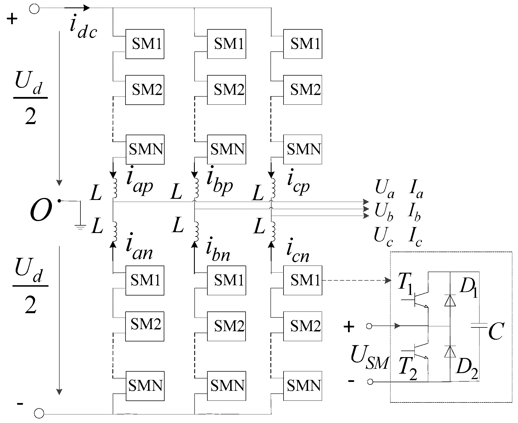
Figure 1 shows a schematic diagram of the main circuit topology of a three-phase MMC. The three-phase leg consists of upper and lower arms, each of which comprises a number of cascaded SMs which are connected in series with an arm inductor. The arm inductor is used to limit fault currents and compensate for the voltage difference between the upper and lower arms [23]. The SM is typically a half-bridge structure with a DC capacitor. As shown in Figure 1, the half-bridge SM consists of two IGBTs (T1 and T2), two antiparallel free-wheeling diode (D1 and D2) and a DC capacitor C.
Obviously, the capacitor of each SM plays the role of a voltage source. According to the operation states of N series-connected SM, an alternating voltage can be generated in each arm, which is composed of N+1 voltage levels. In Figure 1, the and refer to the DC side voltage and current, respectively; , and are the AC side voltages for each phase; , and are the AC side three-phase current; , and are the three-phase upper arm current; , and are the three-phase lower arm currents; is the SM output voltage; and “O” refers to the virtual neutral point of the DC side.
To illustrate the working principle of the MMC, phase A is taken as an example. Note that the phase A arm voltage is , the lower arm voltage is , and the phase A output voltage is . According to the Kirchhoff voltage law, the following equation can be obtained as [2]
To maintain a constant voltage on the DC side, the total number of SMs put into the upper and lower arms of the MMC must remain unchanged at the same time:
where is the number of SMs inserted into the upper arm, is the number of SMs inserted into the lower arm and is the rated voltage of the SM capacitor. Combining Equation (1) and Equation (2), the following equations can be given as Equation (3)
where round (x) denotes the nearest integer to x. Substituting the voltage modulation signal into Equation (3), the number of SMs to be inserted into the upper and lower bridge arms can then be obtained. By controlling the insert or bypass modes of each SM, an AC output voltage close to the target value can be achieved.
The control strategy of the sorting algorithm-based capacitor voltage balancing is to reasonably distribute the switching pulse signals to each SM obtained by the MMC modulation strategy. Under the premise that the output voltage is not changed, the SMs that need to be inserted or bypassed are selected again so as to avoid excessive deviation of the capacitance voltage of each SM on the arm. To clarify the proposed SM capacitor voltage balancing method clearly, the voltage balancing method based on the sorting algorithm and the proposed auto-optimized method are analyzed as follows.
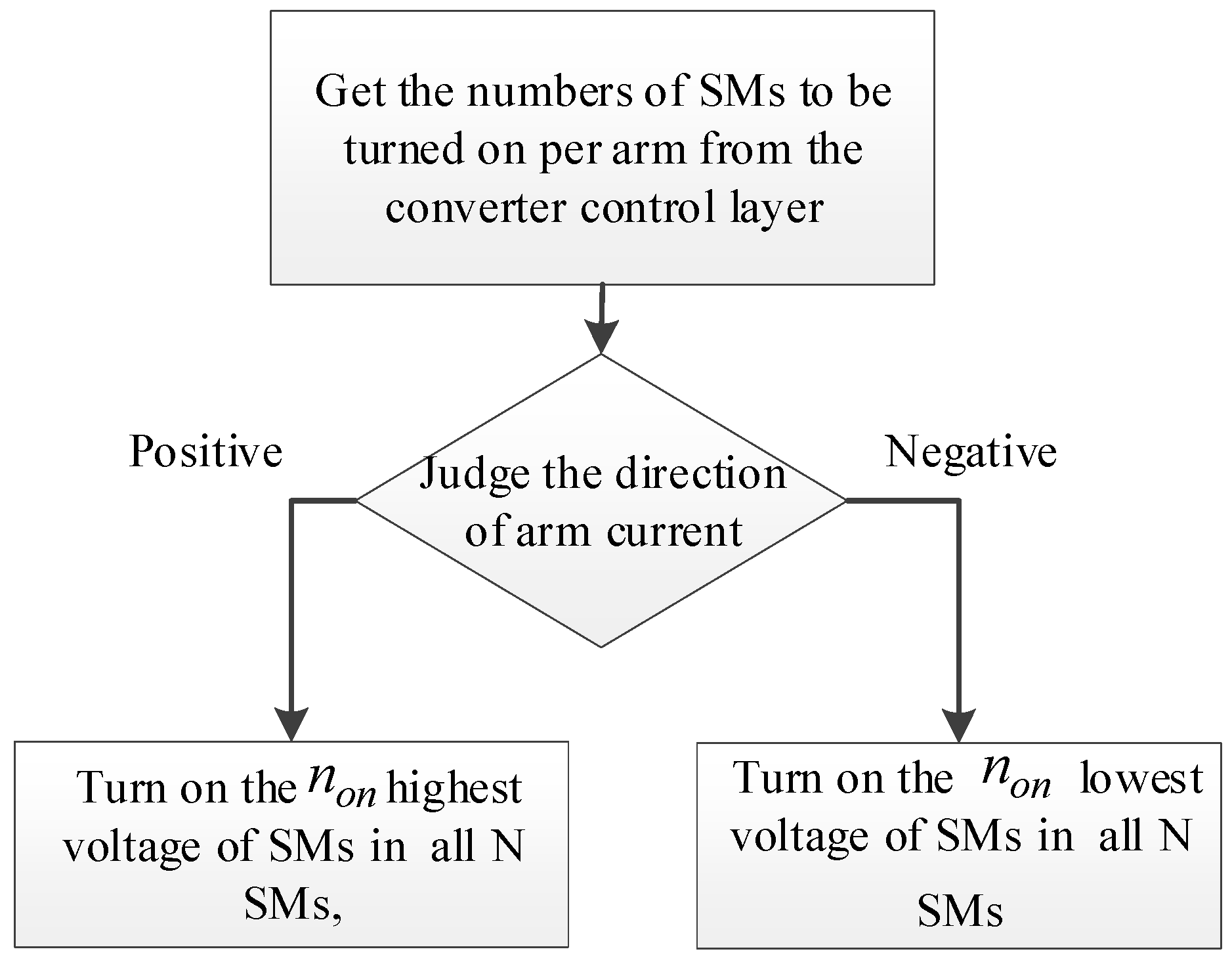
2.2. Sorting Algorithm
First, the number of SMs to be inserted into the arm at a moment is obtained according to the MMC modulation strategy. Then, the direction of the arm current is detected and judged. If the direction of the arm current is positive, the SM in the insert state can absorb the active power to increase the capacitor voltage (charge the capacitor) and the SMs with the lowest capacitor voltage in the arm would be put into operation at present. Conversely, if the direction of the arm current is negative and the inserted SM can release active power (discharge the capacitor), the SMs with the highest capacitor voltage in the arm are switched on.
Because this method does not set the trigger condition for adjusting the switching pulse, the operation state of the SM should be reselected in each trigger cycle. Even if there is only a tiny voltage deviation of the SM capacitors or the total number of inserted SMs remains unchanged, once the sorting result is changed, the switching state of all SMs needs to be adjusted according to the real-time capacitor voltage. This will lead to the unnecessary repeated switching action of an IGBT, which would increase the switching frequency of the device, as well as the switching losses of the MMC.
2.3. The Auto-Optimized SM Capacitor Balancing Algorithm
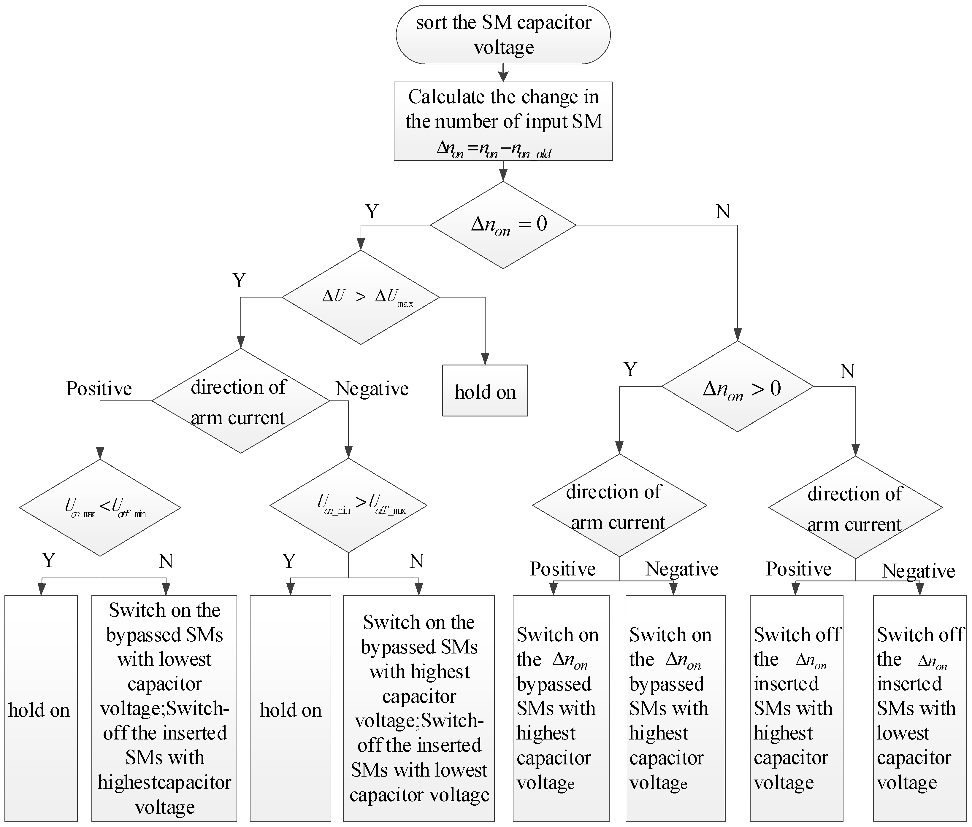
To reduce the switching frequency of the device, this paper proposes an improved voltage sequencing equalization strategy based on the sorting algorithm. By analyzing the switching state of a trigger cycle on the bridge arm SM and the difference between the capacitance voltages of each SM, a new trigger pulse sequence is generated to reduce the switching frequency of the SM. The auto-optimized SM capacitor balancing principle is shown in Figure 3.
The improved voltage sorting voltage equalization algorithm first uses the MMC modulation strategy to obtain the number of SMs that are required to be inserted into the arm in the next cycle, then, subtracts the number of SMs that the arm has been inserted in the previous trigger cycle to obtain inputs, and then, changes the number of SMs in a trigger cycle to the following:
If , more SMs need to be inserted into the arm depending on the direction of the arm current. If the arm current is positive, that is, the SM capacitor is charge with an increased voltage, then the SMs with the lowest capacitor voltage among the previous bypass state SMs will insert into the arm; similarly, if the arm current is negative, that is, the voltage of the inserted SM capacitor will decrease, then the SMs with the highest voltage in the bypass state are switched on. When , the SMs with the highest voltage among the SMs in the previous trigger cycle are bypassed at a positive arm current. The SMs with the lowest voltage among the previously inserted SMs are bypassed at a negative arm current.
In the case of , in order to control the difference between the capacitor voltages of the SMs within a certain range, is defined as the maximum value of the instantaneous capacitor voltages of all SMs in the arm, is defined as the minimum value of the instantaneous capacitor voltages of all SMs in the arm, is the difference between and , and is the maximum voltage deviation threshold, which is preset in advance.
When is less than or equal to , the current trigger pulse is maintained, and the capacitor voltage deviation of the SM is within the allowable range. If is greater than , the direction of arm current is first determined. If the arm current direction is positive, when the maximum voltage of the inserted SM is less than the minimum voltage of the bypassed SM, the existing trigger pulse is maintained; otherwise, the SM with the smallest input capacitor voltage is input, and the SM with the highest capacitor voltage is removed. Similarly, if the arm current is negative, when the minimum value of the voltage in the input SM is greater than the maximum value of the voltage in the SM that has not been input, the existing trigger pulse is maintained; otherwise, the SMs with the highest capacitor voltage are switched on, and the SMs with the lowest capacitor voltage are removed.
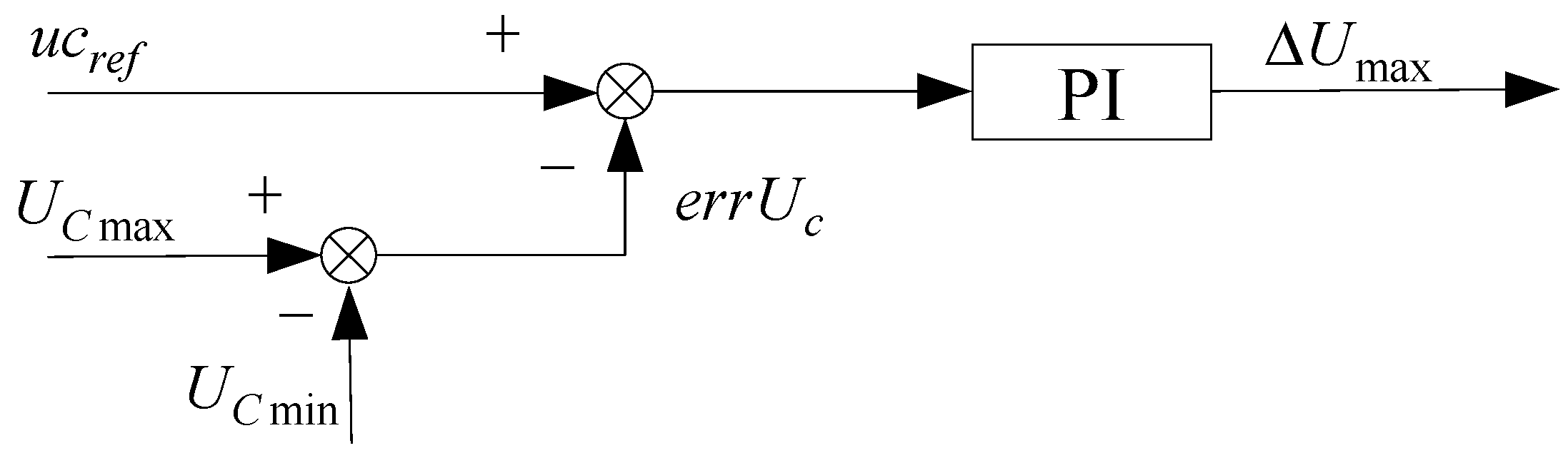
Based on the above analysis, the value of determines the switching frequency and the equalization effect of the whole system. Compared with the fixed value, the dynamic value can lower the system’s switching frequency, and the voltage equalization effect of the bridge wall capacitance is almost the same. A dynamic closed-loop controller is designed as shown in Figure 4. Taking the A-phase upper arm as an example, is the maximum value of the capacitor voltage of all SMs in the A-phase upper arm, and is the minimum value of the capacitor voltage of all SMs in the A-phase upper arm. The difference between the two is the actual deviation of the capacitor voltage . The difference between and the capacitor voltage difference reference value is the input of the proportional integral (PI) control, and the output result is the voltage deviation threshold required for the capacitor voltage equalization.
3. Simulation Verification and Analysis
In order to verify that the auto-optimized capacitor voltage balancing method proposed in this paper is applicable not only to MMC systems with a large number of SMs but also to MMC systems with fewer SMs, a 21-level inverter and 5-level inverter simulation model based on the MMC system are established in Matlab/Simulink.
3.1. 21-Level Inverter Simulation
The simulation has been carried out to verify the performance of the proposed auto-optimized SM capacitor voltage balancing method. A 21-level three-phase MMC model was built in Matlab/Simulink, and tests were conducted on inverter conditions. The simulation parameters are shown in Table 1.
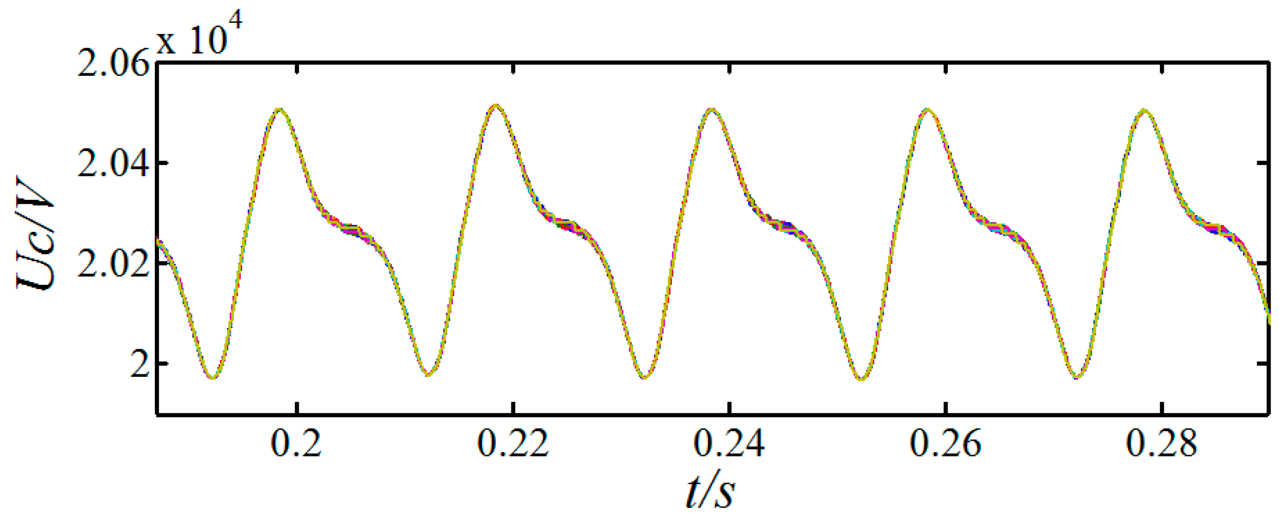
First, the performance of the capacitor voltage balancing algorithm based on sorting is investigated. Figure 5 shows the waveforms of the capacitor voltages of the four SMs at a single phase (e.g., A-phase) upper arm. It can be seen that the SM capacitor voltage remains consistent and their deviation is very small. The fluctuation rate of the voltage amplitude is less than 3%. The average switching frequency of the SM is measured as 2460 Hz.
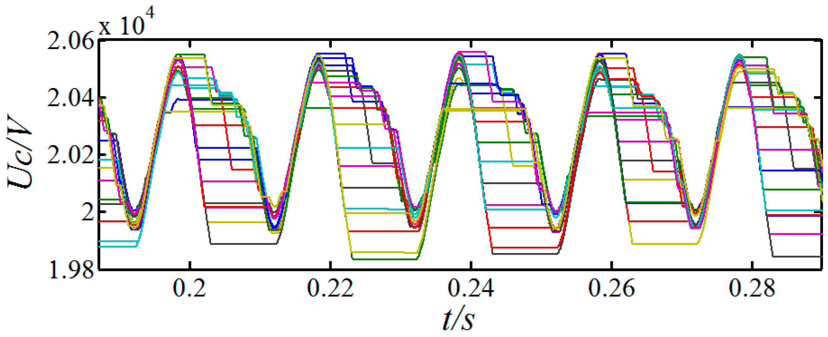
Secondly, in order to highlight the effectiveness of the equalization algorithm, the algorithm of without voltage balancing control is also simulated. The waveform is shown in Figure 6.
Comparing the simulation results between Figure 5 and Figure 6, the without voltage balancing control can greatly reduce the average switching frequency of the IGBT device, e.g., from 2460 Hz to 396 Hz in this case. However, the SM capacitor voltage deviation is also increased, as shown in Figure 6. There is still a certain voltage deviation between the SM capacitance voltages which is unable to meet consistency requirements of capacitance voltages.
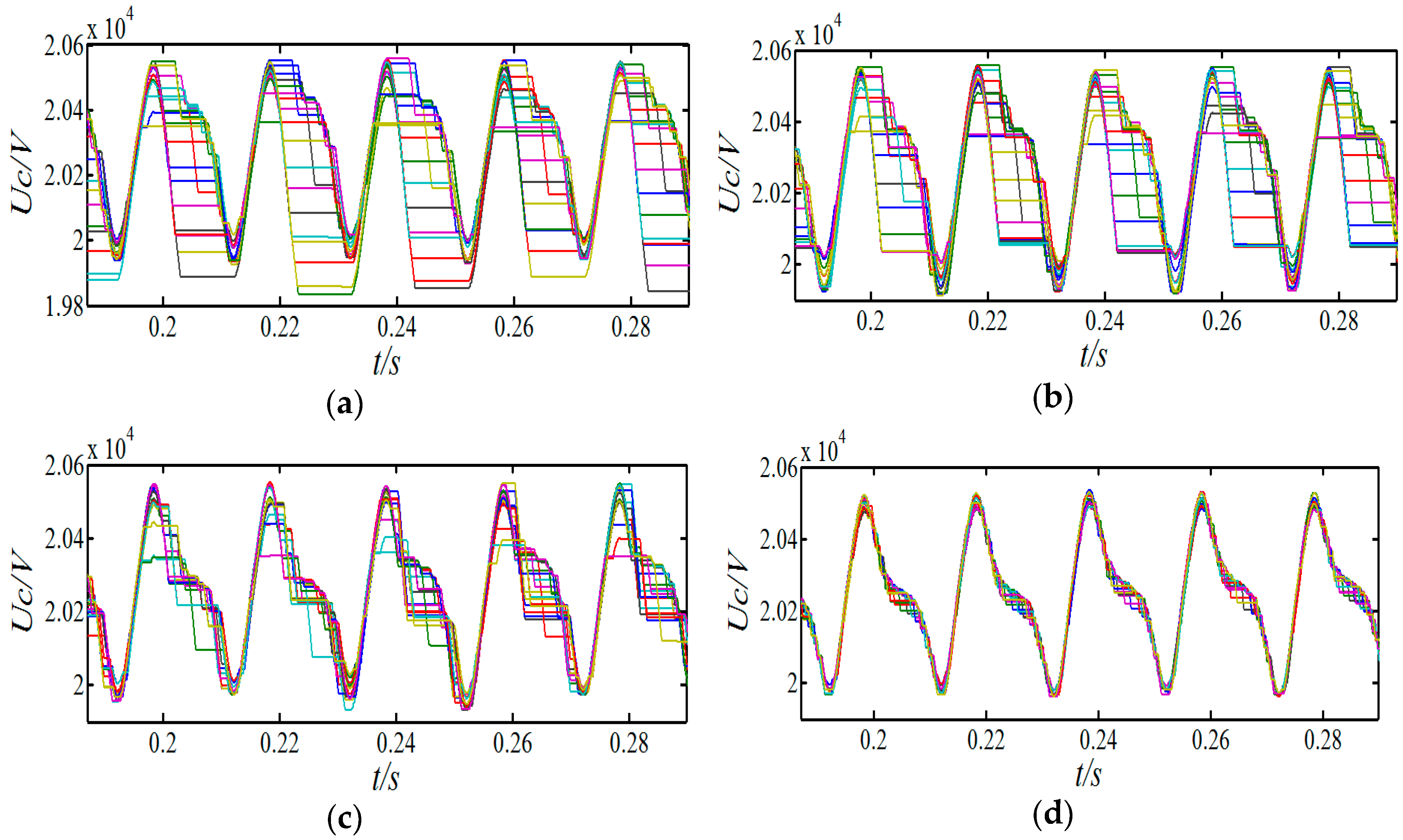
As a comparison, the performance of the proposed auto-optimized voltage balancing algorithm based on the maximum voltage deviation automatic threshold is analyzed. In simulation, the capacitance target deviation are set as 800 V, 500 V, 200 V and 50 V. The waveforms of each upper arm SM capacitor voltages are shown in Figure 7. The SM capacitor voltages still remain stable. In addition, it is observed that, the deviation of the SM capacitor voltages decreases by controlling the capacitance target deviation .
To further compare the performances between the proposed algorithm with the sorting algorithm and the without voltage balancing control algorithm, some metrics are calculated, including the maximum voltage deviation and the average switching frequency. The statistical results are shown in Table 2.
As shown in Table 2, the proposed auto-optimized algorithm can significantly reduce the average switching frequency compared with the sorting algorithm. For example, when the capacitance target deviation is set as 200, the average switching frequency is reduced from 2460 Hz to 462 Hz, which means a reduction of 81%. Compared with the without voltage balancing control, the proposed method can improve the consistency between the SM capacitor voltages by reasonably selecting the capacitance target deviation. Thus, it is possible to prevent excessive voltage deviation from affecting the AC output performance.
3.2. 5-Level Inverter Simulation
In order to enhance and verify the correctness and effectiveness of the proposed optimization algorithm, a 5-level MMC simulation model with 4 SMs is built in Matlab/Simulink. The basic parameters of the system are consistent with the experimental platform parameters. The specific data is shown in Table 3.
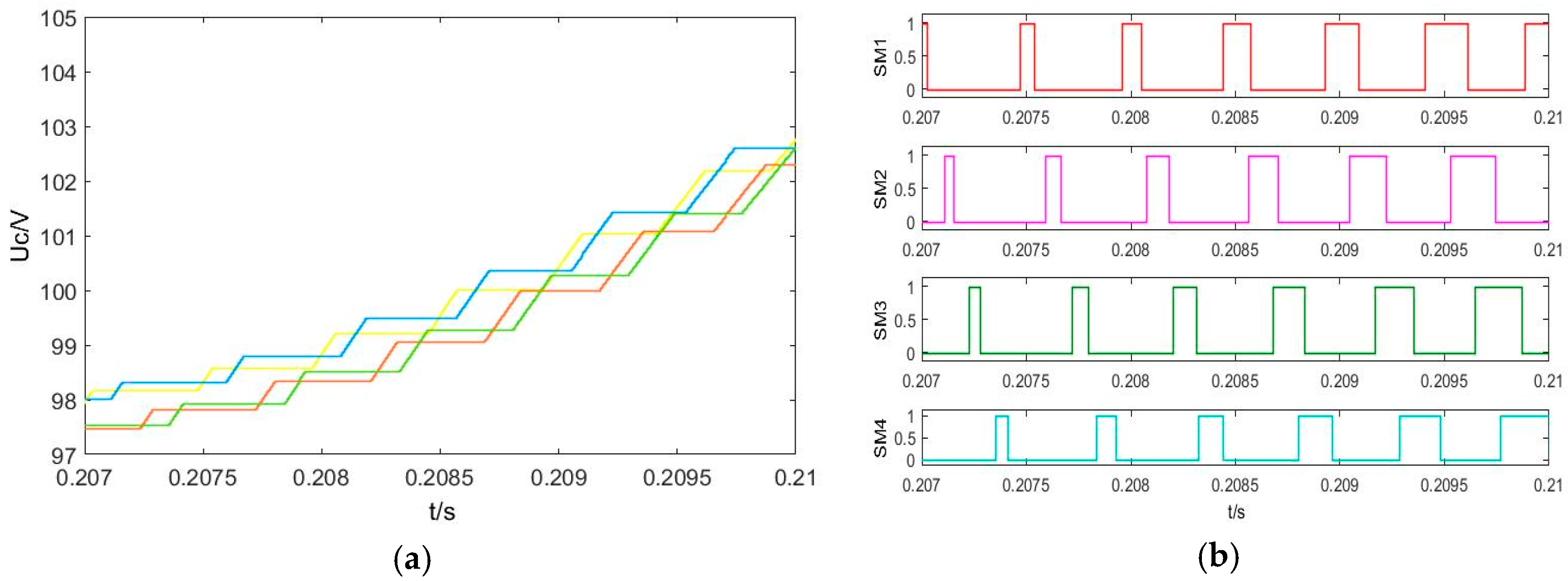
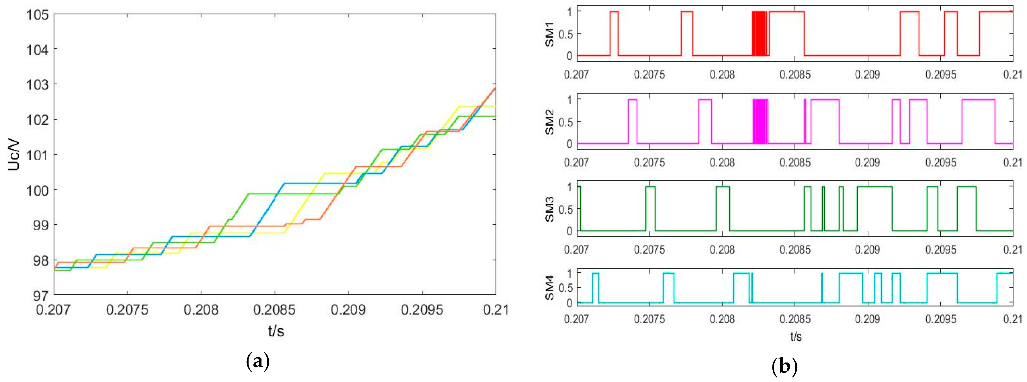
Firstly, the without voltage balancing control is simulated. The simulation results are based on the A-phase upper arm. Figure 8 shows the SM capacitor voltages and trigger pulses. The average switching frequency of the SM is 2050 Hz. The maximum voltage deviation of the SM compared to the rated voltage (100 V) is 4.5 V. The capacitance voltage deviation between SMs is large. Subsequently, the sorting algorithm is simulated. Figure 9 shows the SM capacitor voltages and trigger pulses. The average switching frequency of the SM is 3750 Hz, and the maximum voltage deviation of the SM compared to the rated voltage (100 V) is 2.7 V. The capacitance voltage deviation between SMs is well reduced. However, compared with the without voltage balancing control, the switching frequency is increased by 82.92%.
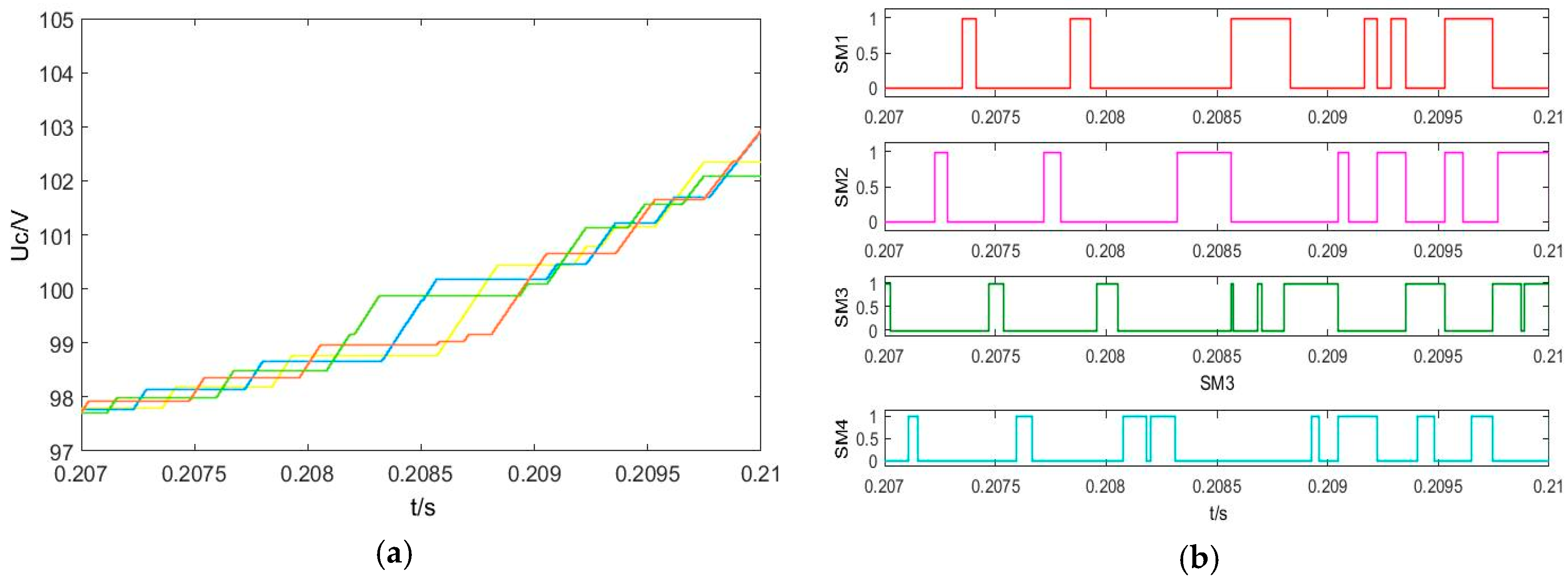
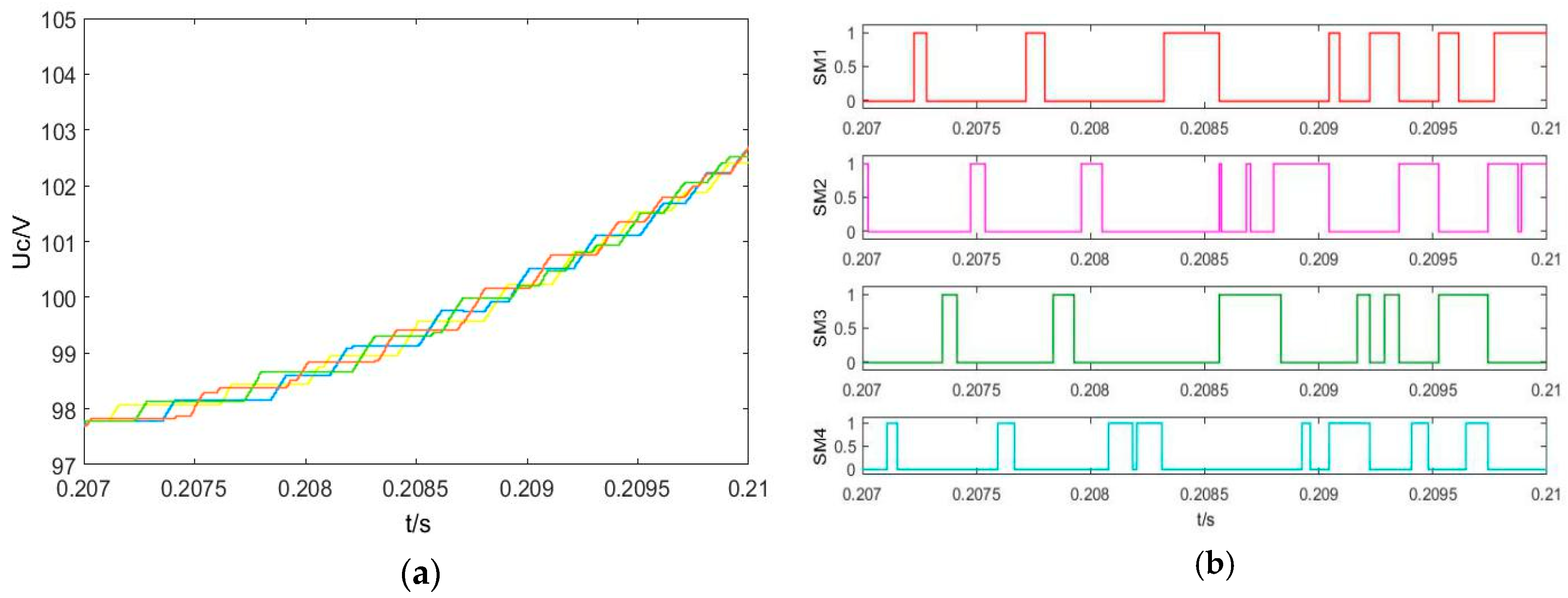
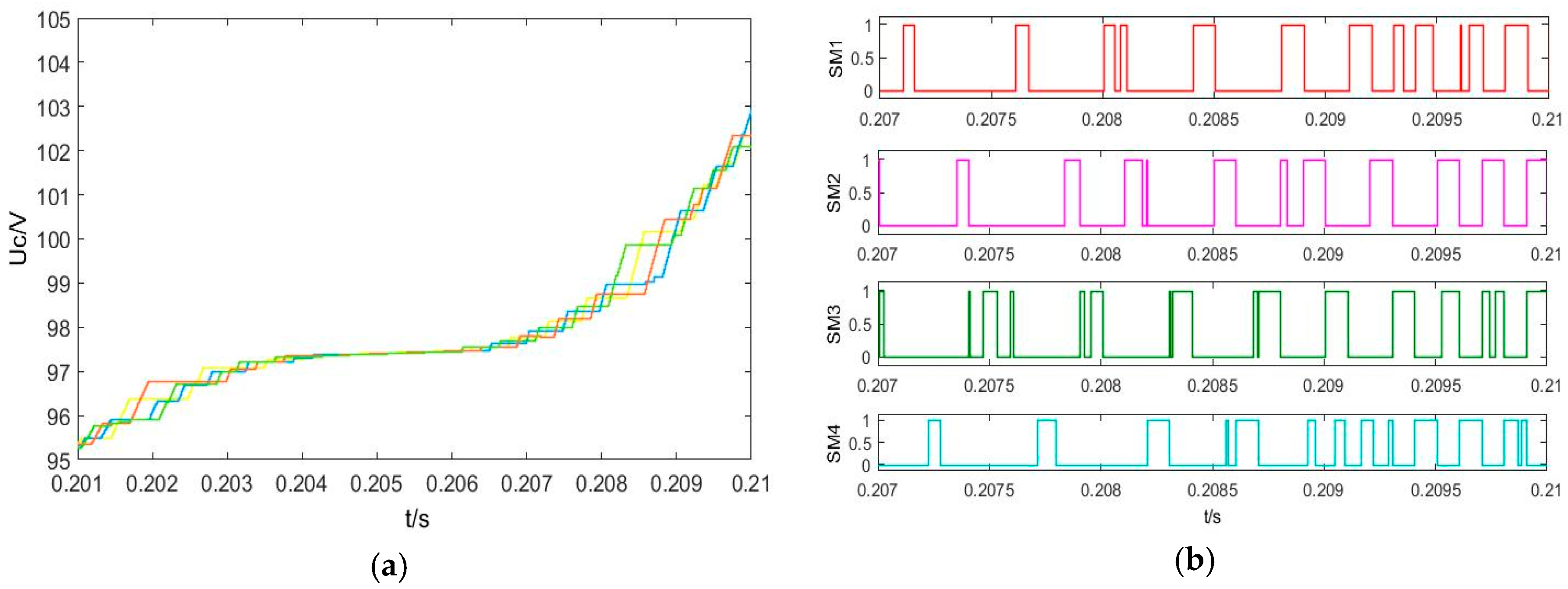
To evaluate the effectiveness of the proposed auto-optimized capacitor voltage balancing method, a different capacitance target deviation was used to control the SM capacitor voltage. Figure 10 shows the SM capacitor voltages and trigger pulses with capacitance target deviation of 5.0 V. The corresponding average switching frequency of the SM is 2060 Hz, and the maximum voltage deviation of the SM compared to the rated voltage (100 V) is 2.6 V. Compared with the former two algorithms, the capacitance voltage deviation between SMs is reduced. The SM capacitor voltage balancing results with the capacitance target deviation of 3.0 V and 0.5 V are shown in Figure 11 and Figure 12, respectively. When the capacitance target deviation is 3.0 V, the corresponding average switching frequency of the SM is 2780 Hz, and the maximum SM voltage deviation compared with the rated voltage (100 V) is 1.7 V. When the capacitance target deviation is 0.5 V, the corresponding average switching frequency of the SM is 3500 Hz, and the capacitance target deviation of the SM compared with the rated voltage (100 V) is 1.0 V. The specific data is shown in Table 4. It can be seen from the comparison of the above experimental results that the auto-optimized equalization algorithm proposed in this paper can not only reduce the capacitance voltage deviation between SMs but also reduce the switching frequency of SMs.
For a better comparison and analysis, the standard deviation between the SM capacitor voltages is defined as the SMs capacitor voltage balance degree, given by
where is the capacitor voltage of the ith SM and is the average of the four capacitor voltages. The difference between the maximum and minimum values among the four SM capacitor voltages divided by the rated voltage of the SM capacitor is defined as the SM capacitor voltage fluctuation rate
where and are the maximum and minimum values of the SMs capacitor voltage, respectively. is the rated voltage of the SM capacitor. To compare the sorting algorithm and the proposed auto-optimized algorithm, the maximum voltage deviation, the average switching frequency, the SM capacitor voltage balance degree and the capacitor voltage fluctuation ratio of SM are calculated. The statistical results are shown in Table 4.
As the simulation data in Table 4, when the capacitance target deviation is 5.0 V, the SM capacitor voltage volatility of the auto-optimized capacitor voltage balancing algorithm proposed in this paper is reduced by 14.4% compared with the sorting algorithm and the total switching frequency is reduced by 45.1%. When the capacitance target deviation is 3.0 V, the SM capacitor voltage volatility is reduced by 27.8% and the total switching frequency is reduced by 26%. When the capacitance target deviation is 0.5 V, the SM capacitor voltage volatility is reduced by 35.2% and the total switching frequency is reduced by 6.7%. Therefore, the deviation threshold algorithm can effectively reduce the capacitance deviation between each SM and the switching frequency appropriately.
4. Experimental Verification and Analysis
Generally speaking, the number of modules in MMCs may be dozens, hundreds, or even thousands, which is used in HVDC systems. The increased number of modules will cause problems such as communication delays and calculations. This paper focuses on the proposed and verified capacitor voltage balance control method under a certain number of modules. Therefore, the number of modules has basically no effect on the simulation and verification of this control method. In the above, the original meaning of this paper is that the 21-level simulation verification shows that the algorithm is applicable to MMC systems with many SMs. The experimental verification of the 5-levels show that the algorithm is also applicable to the MMC system with fewer SMs. Therefore, in order to further verify the auto-optimized capacitor voltage balancing method proposed in this paper, a five-level MMC experimental prototype was established.
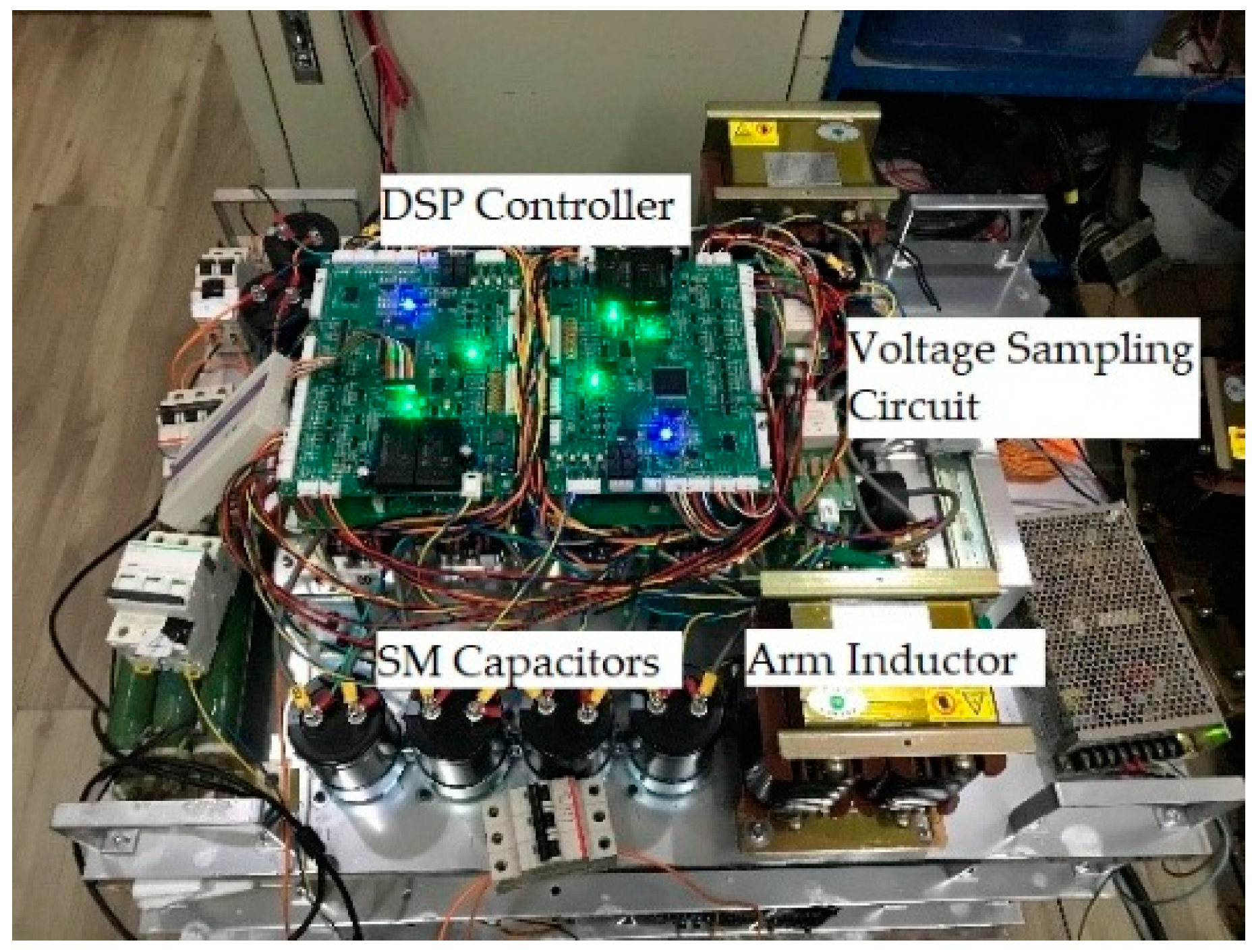
The upper and lower arm experimental setup of a single phase (consist of four SMs per arm) is illustrated in Figure 13. Each half-bridge SMs is built by using Mitsubishi CM100DY-24 A IGBT modules (1200 V/100 A, Mitsubishi Electric, Tokyo, Japan), whilst the SM capacitors are the EPCOS 2200 uF/450 V electrolytic capacitor (TDK Electronics AG, Munich, Germany). The proposed algorithm for single phase, i.e., per leg, is implemented by the Texas DSP TMS320F28335 with 150 MHz operating frequency. Such a controller has a 12-bit ADC module with 16-channels, which are adequate to sense the SM capacitor voltages and arm current.
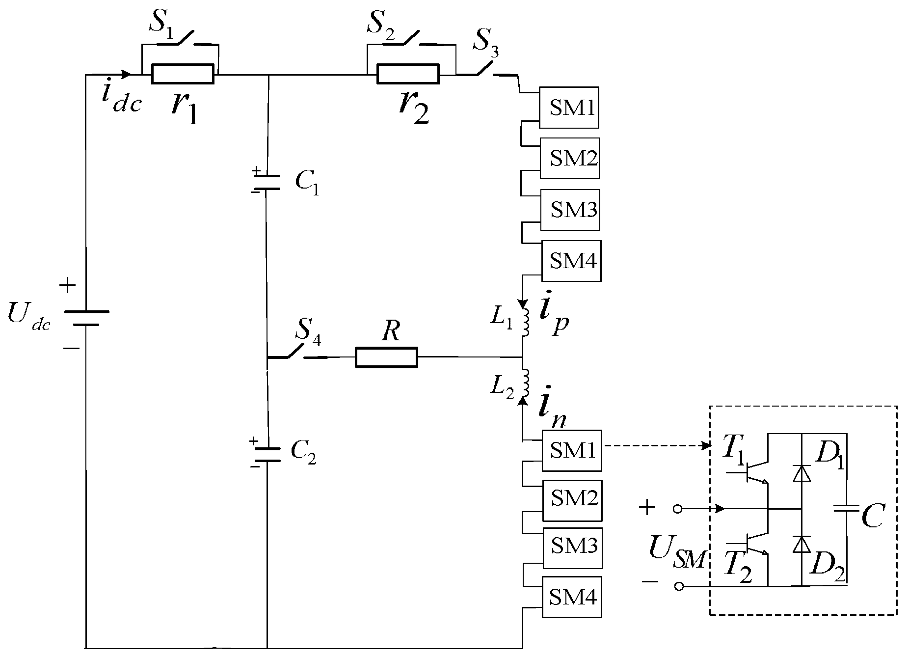
The topology of the experimental platform is shown in Figure 14. In the control of the MMC capacitor voltage, in addition to the voltage equalization control of the sub-module during the steady state, it is necessary to perform a reasonable pre-charge control at the start of the MMC so that the capacitor voltage value reaches the rated value Udc/N that meets the normal working requirements to ensure that the system enters the normal operation phase safely and smoothly. Reference [27] gives the principle of pre-charging and its specific process. The experimental platform first disconnects the switches S1, S2, S3 and S4. Then, the DC bus terminal charges the two capacitors C1 and C2 connected in parallel at the DC bus terminal through the resistor r1 so that the voltage across the capacitor reaches the rated value Udc/2. Taking the capacitor charging of the above bridge arm sub-module as an example, the switch S3 and the switch S1 are closed and the IGBT in the bridge arm sub-module is controlled by the DSP so that the upper arm sub-module is in the input state and the lower-arm sub-module is in the resected state. At this time, the DC bus terminal charges the capacitor of the upper arm SM through the resistor r2 to reach the rated value Udc/N. The lower arm SM capacitor is charged as above. More details of the experiment parameters are shown in Table 5.
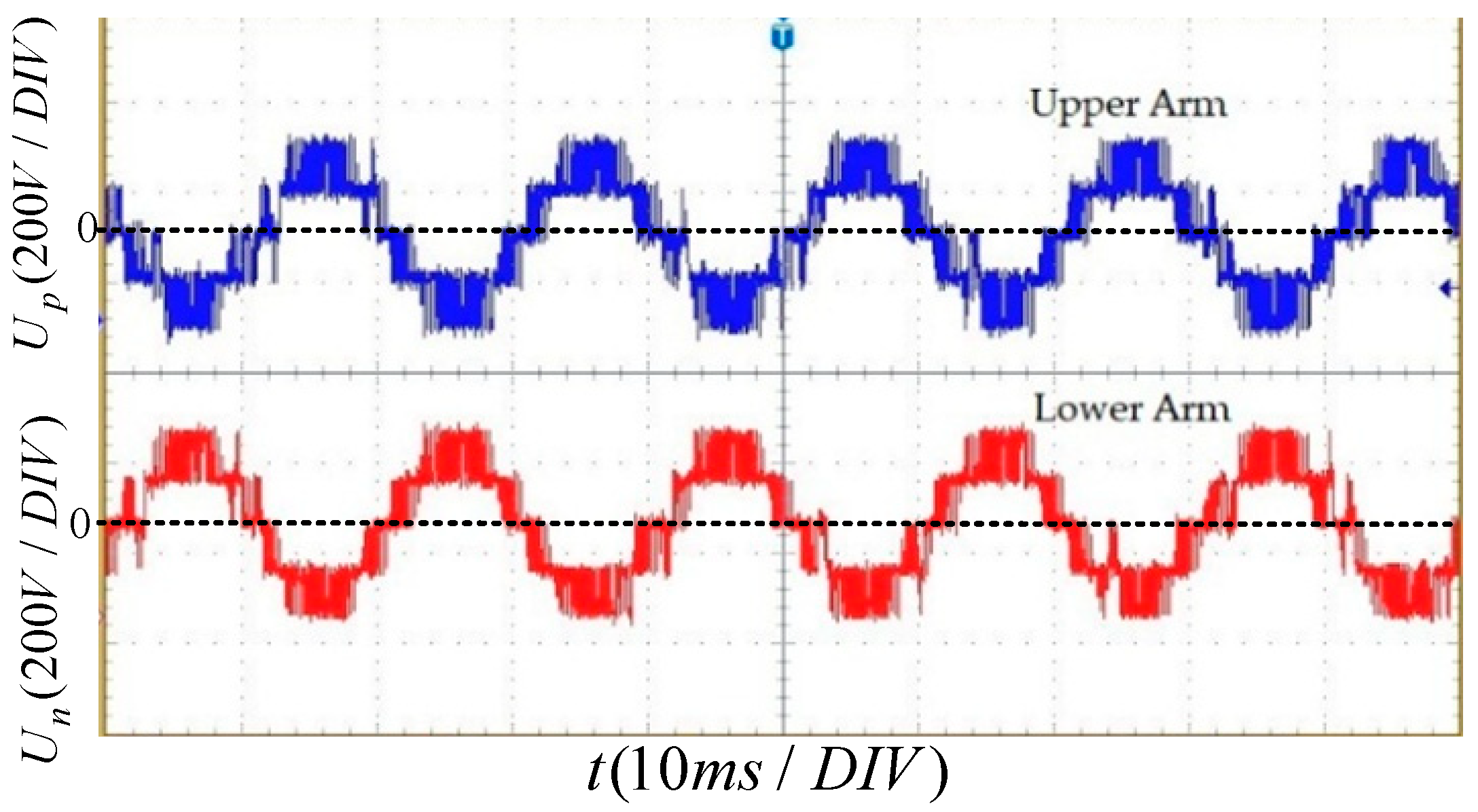
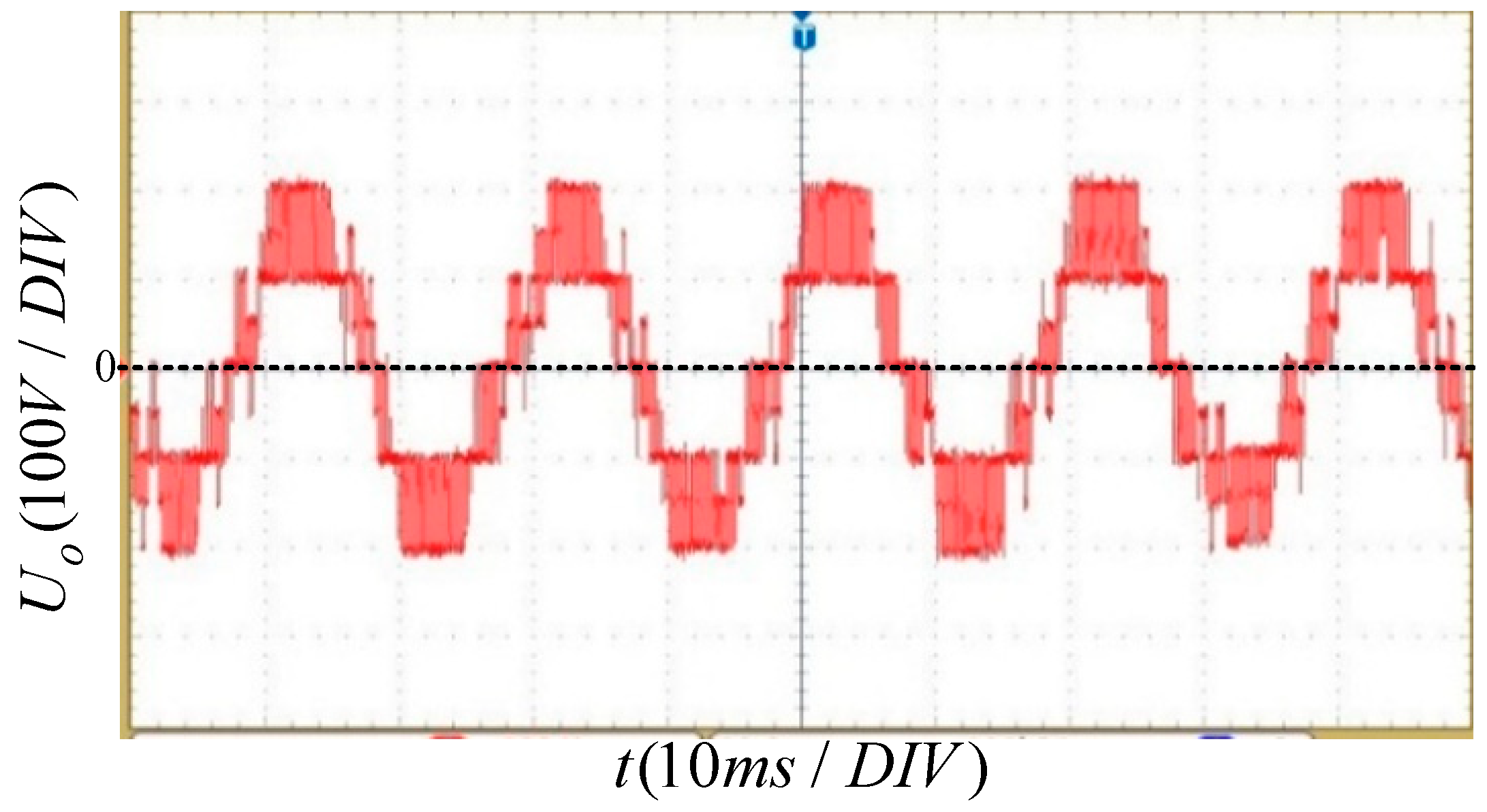
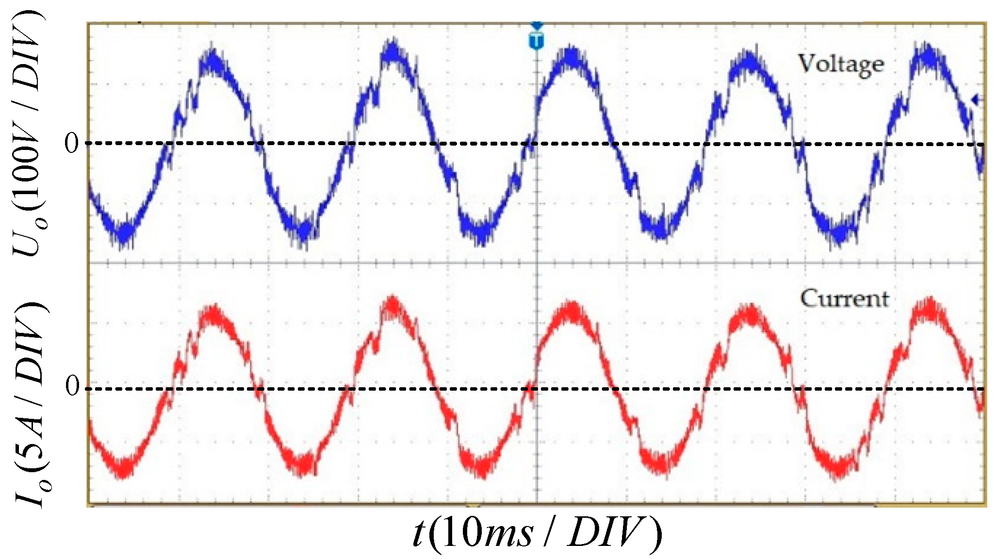
The five-level output voltage waveforms of the upper and lower bridge arms and the single phase MMC with no load are shown in Figure 15 and Figure 16 respectively. Figure 17 shows the 50 Hz sinusoidal output voltage and current waveforms of the single phase MMC with a 25 Ω resistance load. As shown in Figure 16, when there is no resistance on the AC output side, the output side voltage level is five. As shown in Figure 17, when a purely resistive load is applied to the output side without filtering mean, the sinusoidal voltage current waveform can be obtained on the output side. Therefore, these results indicate a good output performance of the MMC.
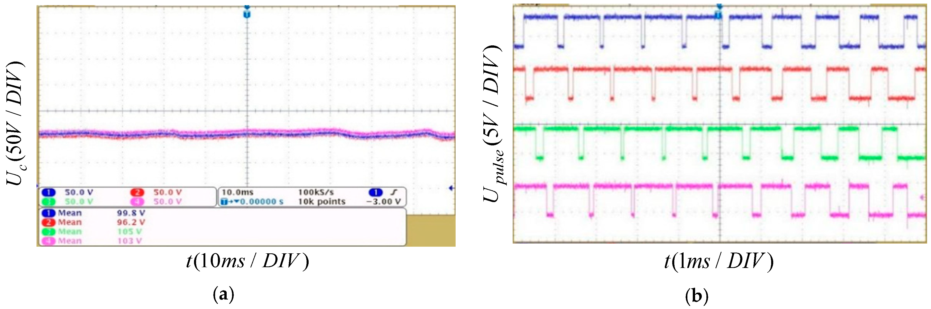
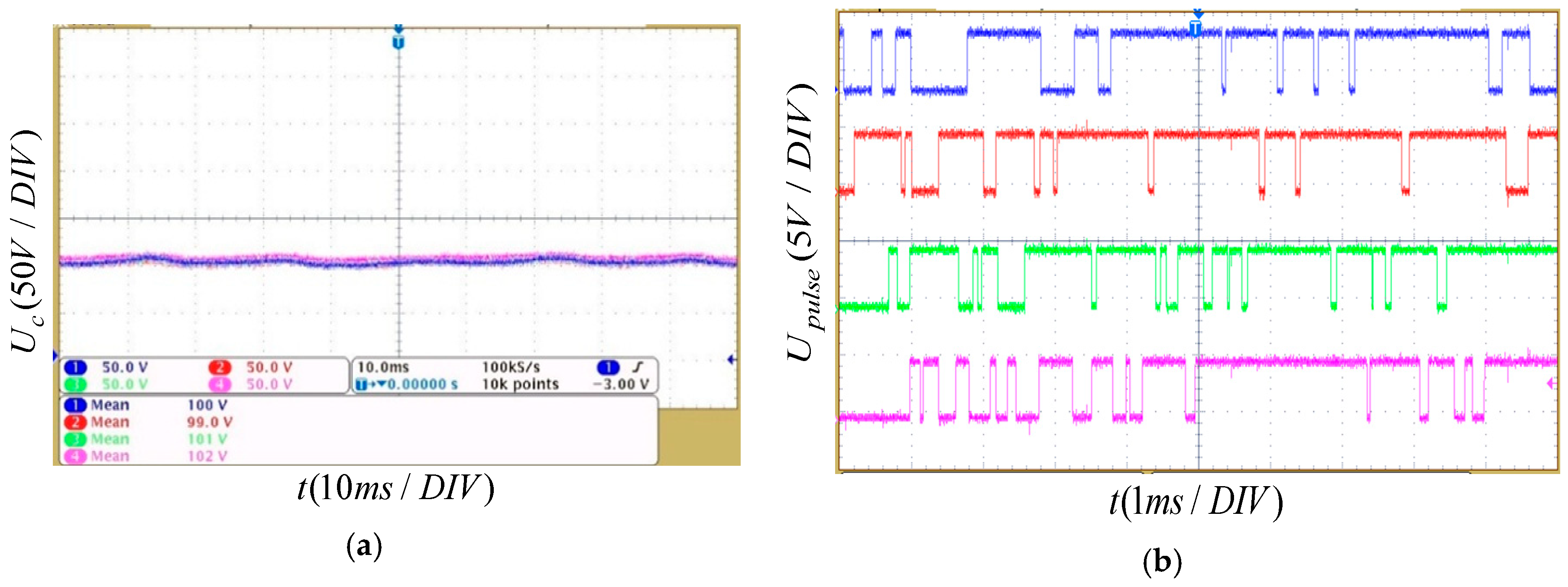
Figure 18 shows the four SM capacitor voltages waveforms of the upper arm and the trigger pulse of the SMs without voltage balancing control. It can be seen that the corresponding average switching frequency of the SMs is 2100 Hz, and the SM maximum voltage deviation compared with the rated voltage (100 V) is 5.0 V. The voltage amplitudes of the SMs are quite inconsistent. Figure 19 shows the waveforms of the SM capacitor voltages and the trigger pulse of the SMs by the sorting algorithm. The deviation between the four SM capacitor voltages is well controlled. However, the average switching frequency of the SMs is 3800 Hz, which is an increase of 81% compared with the switching frequency without voltage balancing control. The above results show that the sorting algorithm can reduce the deviation between SM capacitor voltages, but the switching frequency and switching loss of the MMC system is also increased.
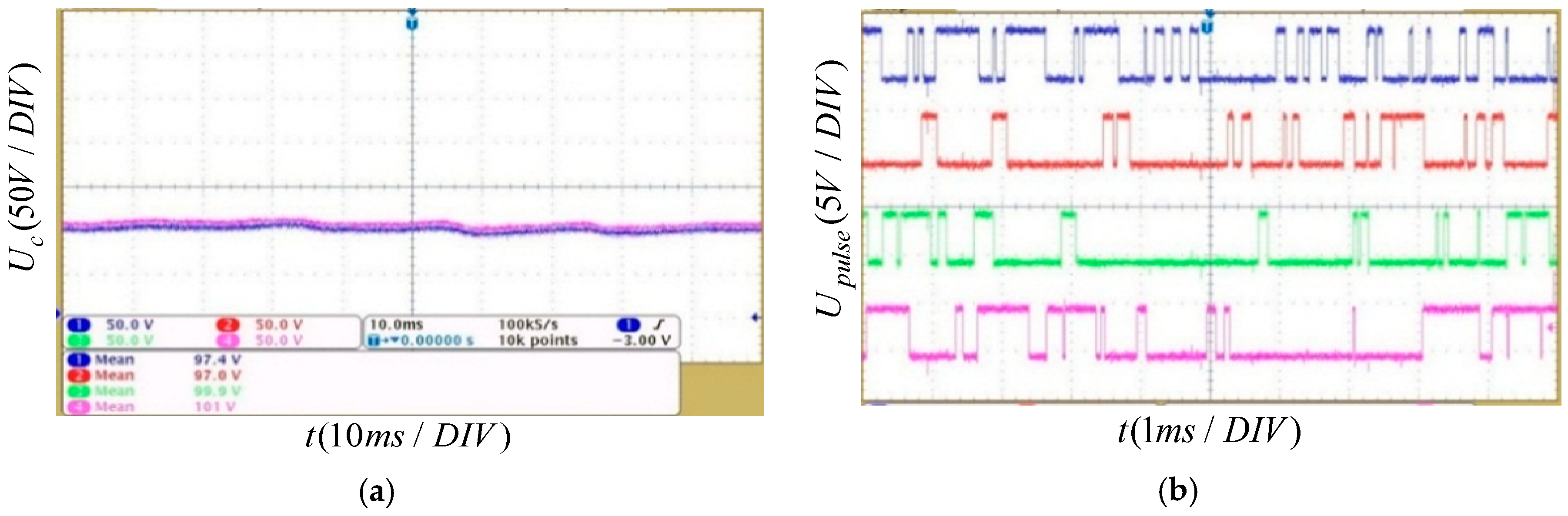
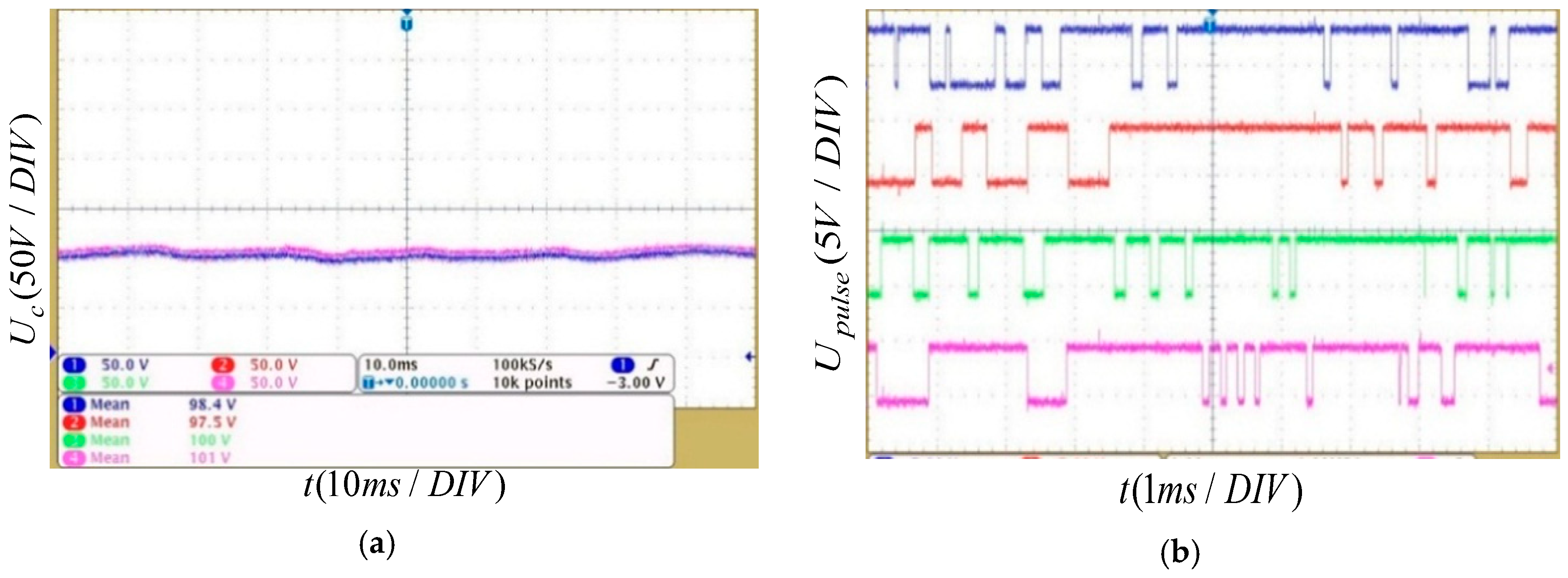
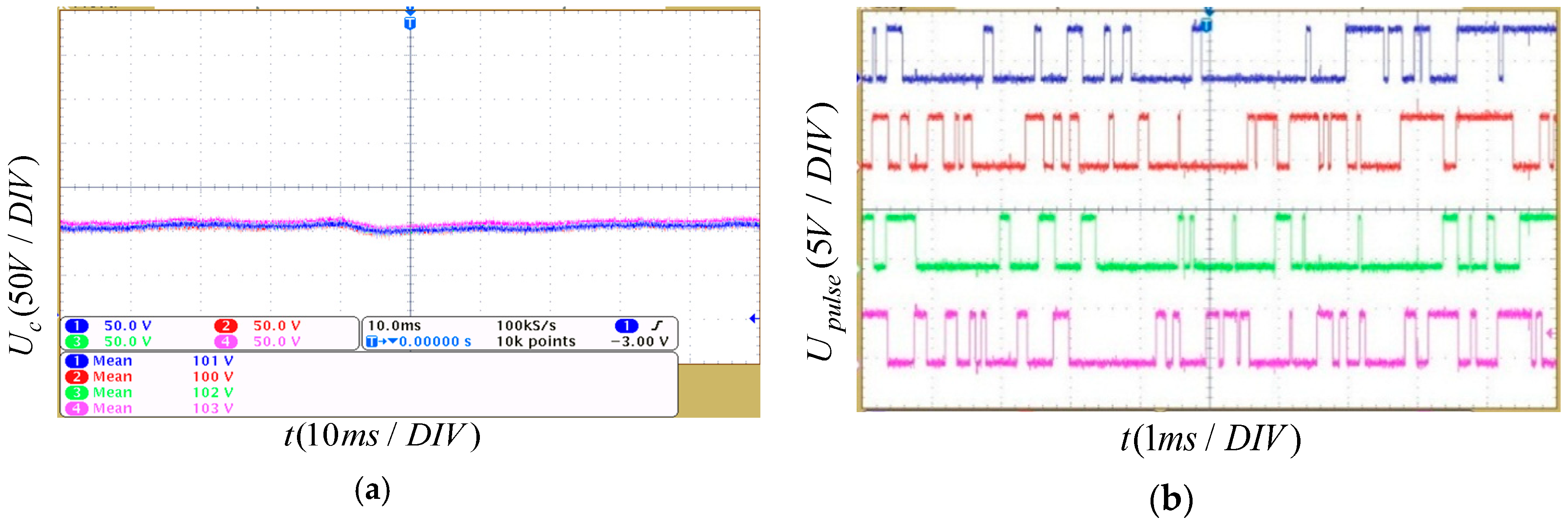
In order to evaluate effectiveness of the proposed voltage balancing algorithm, the different capacitance target deviations were used to control the SM capacitor voltages. Figure 20 shows the SM capacitor voltages and trigger pulses with a capacitance target deviation of 5.0 V. It is seen that the SM capacitor voltages keep stable around the rated value with a high degree of consistency. Moreover, the SM capacitor voltage balancing results with the capacitance target deviation of 3.0 V and 0.5 V are shown in Figure 21 and Figure 22, respectively. Similarly, it is seen that the deviation between the SM capacitor voltages decreases by controlling the capacitance target deviation. In other words, the consistency of each SM capacitor voltages is improved with a capacitance target deviation, which conforms to the simulation results.
To compare the sorting algorithm and the proposed auto-optimized algorithm, the maximum voltage deviation, the average switching frequency, the SM capacitor voltage balance degree and the capacitor voltage fluctuation ratio of SM are calculated. The statistical results are shown in Table 6.
As shown in Table 6, the experimental results verify that when the capacitance target deviation is 5.0 V, the SM capacitor voltage volatility of the dynamic deviation threshold algorithm proposed in this paper is reduced by 12.5% compared with the sorting algorithm and the total switching frequency is reduced by 43.4%. When the capacitance target deviation is 3.0 V, the SM capacitor voltage volatility is reduced by 25% and the total switching frequency is reduced by 32.4%. When the capacitor target deviation is 0.5 V, the SM capacitor voltage volatility is reduced by 30% and the total switching frequency is reduced by 6%. The dynamic deviation threshold algorithm can effectively reduce the capacitance deviation between each SM and the switching frequency appropriately.
5. Conclusions
This paper analyzes the topology and operation principle of MMC and proposes an auto-optimized capacitor voltage balancing method. Considering the switching state of the switch on the SM and the difference between the voltages of the SMs, the switching frequency of the MMC SM is reduced by the balancing optimization algorithm of the dynamic voltage deviation threshold.
The 21-level simulation shows that when the capacitance target deviation is changed from 200 V to 500V, the switching frequency can always be reduced by more than 81.3% compared with the sorting algorithm. The 5-level simulation shows that when the capacitance target deviation is 5.0 V, the SM capacitor voltage volatility of the auto-optimized capacitor voltage balancing algorithm is reduced by 14.4% compared with the sorting algorithm and the total switching frequency is reduced by 45.1%. The experimental results verify that when the capacitance target deviation is 5.0 V, the SM capacitor voltage volatility of the dynamic deviation threshold algorithm proposed in this paper is reduced by 12.5% compared with the sorting algorithm and the total switching frequency is reduced by 43.4%.
Therefore, the proposed auto-optimized capacitor voltage balancing control strategy of the MMC SM can maintain the overall stability while reducing the switching losses of the system.
Author Contributions
Conceptualization, J.Z. and R.L.; methodology, J.Z. and C.K.; software, C.K.; validation, J.Z., C.K. and T.L.; formal analysis, J.Z. and C.K.; investigation, T.L. and R.L.; resources, J.Z. and R.L.; data curation, C.K.; writing—original draft preparation, J.Z. and R.L.; writing—review and editing, J.Z., C.K. and R.L.; visualization, C.K.; supervision, T.L.; project administration, J.Z.
Funding
This research was supported by 111 project, No. D18003.
Conflicts of Interest
The authors declare no conflict of interest.
References
- Anton, L.; Rainer, M. An innovative modular multilevel converter topology suitable for a wide power range. In Proceedings of the IEEE Power Tech Conference Proceedings, Bologna, Italy, 23–26 June 2003; Volume 3, pp. 1–6. [Google Scholar]
- Suman, D.; Jiangchao, Q.; Behrooz, B.; Maryam, S.; Peter, B. Operation, Control, and Applications of the Modular Multilevel Converter: A Review. IEEE Trans. Power Electron. 2015, 30, 37–53. [Google Scholar]
- Kim, C.; Lee, S. Redundancy Determination of HVDC MMC Modules. Electronics 2015, 4, 526–537. [Google Scholar] [CrossRef] [Green Version]
- Lu, J.; Huang, Q.; Mao, X.; Tan, Y.; Zhu, S.; Zhu, Y. Optimized Design of Modular Multilevel DC De-Icer for High Voltage Transmission Lines. Electronics 2018, 7, 204. [Google Scholar] [CrossRef]
- Han, X.; Sima, W.; Yang, M.; Li, L.; Yuan, T.; Si, Y. Transient Characteristics Under Ground and Short-Circuit Faults in a ±500 kV MMC-Based HVDC System with Hybrid DC Circuit Breakers. IEEE Trans. Power Deliv. 2018, 33, 1378–1387. [Google Scholar] [CrossRef]
- Jing, L.; Xu, C.; Marta, M. Frequency Domain Stability Analysis of MMC-Based HVDC for Wind Farm Integration. IEEE J. Emerg. Sel. Top. Power Electron. 2016, 4, 141–151. [Google Scholar]
- Mehrasa, M.; Pouresmaeil, E.; Zabihi, S.; Catalão, J.P.S. Dynamic Model, Control and Stability Analysis of MMC in HVDC Transmission Systems. IEEE Trans. Power Deliv. 2017, 32, 1471–1482. [Google Scholar] [CrossRef]
- Wickramasinghe, H.R.; Konstantinou, G.; Pou, J.; Agelidis, V.G. Interactions Between Indirect DC-Voltage Estimation and Circulating Current Controllers of MMC-Based HVDC Transmission Systems. IEEE Trans. Power Syst. 2018, 33, 829–838. [Google Scholar] [CrossRef]
- Mehrasa, M.; Pouresmaeil, E.; Zabihi, S.; Vechiu, I.; Catalão, J. A multi-loop control technique for the stable operation of modular multilevel converters in HVDC transmission systems. Int. J. Electr. Power Energy Syst. 2018, 96, 194–207. [Google Scholar] [CrossRef]
- Mehrasa, M.; Pouresmaeil, E.; Taheri, S.; Vechiu, I. Novel Control Strategy for Modular Multilevel Converters Based on Differential Flatness Theory. IEEE J. Emerg. Sel. Top. Power Electron. 2018, 6, 888–897. [Google Scholar] [CrossRef]
- Mehrasa, M.; Pouresmaeil, E.; Akorede, M.; Zabihi, S.; Catalão, J. Function-based modulation control for modular multilevel converters under varying loading and parameters conditions. IET Gener. Transm. Distrib. 2016, 11, 3222–3230. [Google Scholar] [CrossRef]
- Du, S.; Wu, B.; Zargari, N. Delta-Channel Modular Multilevel Converter for a Variable-Speed Motor Drive Application. IEEE Trans. Ind. Electron. 2018, 65, 6131–6139. [Google Scholar] [CrossRef]
- Li, B.; Zhou, S.; Xu, D.; Finney, S.J.; Williams, B.W. A Hybrid Modular Multilevel Converter for Medium-Voltage Variable-Speed Motor Drives. IEEE Trans. Power Electron. 2017, 32, 4619–4630. [Google Scholar] [CrossRef] [Green Version]
- Wu, L.; Qin, J.; Hao, Q.; Saeedifard, M.; Wasynczuk, O.; Shenai, K. Efficiency Evaluation of the Modular Multilevel Converter Based on Si and SiC Switching Devices for Medium/High-Voltage Applications. IEEE Trans. Electron. Devices. 2015, 62, 286–293. [Google Scholar] [CrossRef]
- Allebrod, S.; Hamerski, R.; Marquardt, R. New transformerless, scalable Modular Multilevel Converters for HVDC-transmission. In Proceedings of the IEEE Power Electronics Specialists Conference, Rhodes, Greece, 15–19 June 2008; Volume 3, pp. 174–179. [Google Scholar]
- Wu, D.; Peng, L. Analysis and Suppressing Method for the Output Voltage Harmonics of Modular Multilevel Converter. IEEE Trans. Power Electron. 2016, 31, 4755–4765. [Google Scholar] [CrossRef]
- Fehr, H.; Gensior, A.; Müller, M. Analysis and Trajectory Tracking Control of a Modular Multilevel Converter. IEEE Trans. Power Electron. 2015, 30, 398–407. [Google Scholar] [CrossRef]
- Gilbert, B.; Erik, B.; Philippe, E.; Pierre, L.; Amir, A.; Jean-Claude, V.; Marta, M. An Energy-Based Controller for HVDC Modular Multilevel Converter in Decoupled Double Synchronous Reference Frame for Voltage Oscillation Reduction. IEEE Trans. Ind. Electron. 2013, 60, 2360–2371. [Google Scholar]
- Huang, J.; Wu, T.; Wang, K. Modular Multi-level Converter Control Method Based on CPS—PWM. In Proceedings of the 2017 International Conference on Computer Systems, Electronics and Control (ICCSEC), Dalian, China, 25–27 December 2017; pp. 1528–1531. [Google Scholar]
- Dekka, A.; Wu, B.; Zargari, N.R.; Fuentes, R.L. Dynamic Voltage Balancing Algorithm for Modular Multilevel Converter: A Unique Solution. IEEE Trans. Power Electron. 2016, 31, 952–963. [Google Scholar] [CrossRef]
- Adam, G.P.; Anaya-Lara, O.; Burt, G.M.; Telford, D.; Williams, B.W.; McDonald, J.R. Modular multilevel inverter: Pulse width modulation and capacitor balancing technique. IET Power Electron. 2010, 3, 702–715. [Google Scholar] [CrossRef]
- Tu, Q.; Xu, Z.; Lie, X. Reduced switching-frequency modulation and circulating current suppression for modular multilevel converters. IEEE Trans. Power Del. 2011, 26, 2009–2017. [Google Scholar]
- Jiangchao, Q.; Saeedifard, M. Reduced switching-frequency voltagebalancing strategies for modular multilevel HVDC converters. IEEE Trans. Power Del. 2013, 28, 2403–2410. [Google Scholar]
- Luo, Y.; Li, Y.; Li, Z.; Wang, P.; Xu, F.; Liu, J. Analysis and calculation of the power device switching frequency of modular multilevel converters. In Proceedings of the 2014 9th IEEE Conference on Industrial Electronics and Applications, Hangzhou, China, 9–11 June 2014; pp. 908–912. [Google Scholar]
- Qiu, J.; Dai, T.; Cui, Y. Research on capacitance voltage balance of modular multilevel converter based on improved quick sorting method. In Proceedings of the 2017 Chinese Automation Congress (CAC), Jinan, China, 20–22 October 2017; pp. 5608–5612. [Google Scholar]
- Hofmann, V.; Bakran, M. A capacitor voltage balancing algorithm for hybrid modular multilevel converters in HVDC applications. In Proceedings of the 2017 IEEE 12th International Conference on Power Electronics and Drive Systems (PEDS), Honolulu, HI, USA, 12–15 December 2017; pp. 691–696. [Google Scholar]
- Li, B.; Xu, D.; Zhang, Y.; Yang, R.; Wang, G.; Wang, W.; Xu, D. Closed-Loop Precharge Control of Modular Multilevel Converters During Start-Up Processes. IEEE Trans. Power Electron. 2015, 30, 4755–4765. [Google Scholar] [CrossRef]
Figure 1.
Schematic diagram of the three-phase Modular Multilevel Converter (MMC) structure.

Figure 2.
Flowchart of the sorting algorithm.

Figure 3.
Flowchart of the proposed sub-module (SM) capacitor voltage balancing algorithm.

Figure 4.
Dynamic closed loop controller.

Figure 5.
The waveforms of the SM capacitor voltages of a single phase by the sorting algorithm (SM 1 to SM 20).
Figure 5.
The waveforms of the SM capacitor voltages of a single phase by the sorting algorithm (SM 1 to SM 20).

Figure 6.
The waveforms of the SM capacitor voltages (SM 1 to SM 20) of a single phase without voltage balancing control.
Figure 6.
The waveforms of the SM capacitor voltages (SM 1 to SM 20) of a single phase without voltage balancing control.

Figure 7.
The waveforms of the SM capacitor voltages by the auto-optimized capacitor voltage balancing algorithm (SM 1 to SM 20). (a) is 800 V, (b) is 500 V, (c) is 200 V, and (d) is 50 V.
Figure 7.
The waveforms of the SM capacitor voltages by the auto-optimized capacitor voltage balancing algorithm (SM 1 to SM 20). (a) is 800 V, (b) is 500 V, (c) is 200 V, and (d) is 50 V.

Figure 8.
SM capacitor voltages and trigger pulses without voltage balancing control. (a) SM capacitor voltages of the upper arm. (b) Trigger pulse of the SMs.
Figure 8.
SM capacitor voltages and trigger pulses without voltage balancing control. (a) SM capacitor voltages of the upper arm. (b) Trigger pulse of the SMs.

Figure 9.
SM capacitor voltage balancing results using sorting algorithm. (a) SM capacitor voltages of the upper arm. (b) Trigger pulse of the SMs.
Figure 9.
SM capacitor voltage balancing results using sorting algorithm. (a) SM capacitor voltages of the upper arm. (b) Trigger pulse of the SMs.

Figure 10.
SM capacitor voltage balancing results using the proposed auto-optimized algorithm (Capacitance target deviation is 5.0 V). (a) SM capacitor voltages of the upper arm. (b) Trigger pulse of the SMs.
Figure 10.
SM capacitor voltage balancing results using the proposed auto-optimized algorithm (Capacitance target deviation is 5.0 V). (a) SM capacitor voltages of the upper arm. (b) Trigger pulse of the SMs.

Figure 11.
SM capacitor voltage balancing results using the proposed auto-optimized algorithm (Capacitance target deviation is 3.0 V). (a) SM capacitor voltages of the upper arm. (b) Trigger pulse of the SMs.
Figure 11.
SM capacitor voltage balancing results using the proposed auto-optimized algorithm (Capacitance target deviation is 3.0 V). (a) SM capacitor voltages of the upper arm. (b) Trigger pulse of the SMs.

Figure 12.
SM capacitor voltage balancing results using the proposed auto-optimized algorithm (Capacitance target deviation is 0.5 V). (a) SM capacitor voltages of the upper arm. (b) Trigger pulse of the SMs.
Figure 12.
SM capacitor voltage balancing results using the proposed auto-optimized algorithm (Capacitance target deviation is 0.5 V). (a) SM capacitor voltages of the upper arm. (b) Trigger pulse of the SMs.

Figure 13.
Experimental setup of a five-level single phase MMC.

Figure 14.
Experimental device topology.

Figure 15.
Output voltage results of the upper and lower bridge arms with no load.

Figure 16.
Output voltage results of the single phase MMC with no load.

Figure 17.
Output voltage and current results of the single phase MMC with a load.

Figure 18.
SM capacitor voltages and trigger pulses without voltage balancing control. (a) SM capacitor voltages of the upper arm. (b) Trigger pulse of the SMs.
Figure 18.
SM capacitor voltages and trigger pulses without voltage balancing control. (a) SM capacitor voltages of the upper arm. (b) Trigger pulse of the SMs.

Figure 19.
SM capacitor voltage balancing results using sorting algorithm. (a) SM capacitor voltages of the upper arm. (b) Trigger pulse of the SMs.
Figure 19.
SM capacitor voltage balancing results using sorting algorithm. (a) SM capacitor voltages of the upper arm. (b) Trigger pulse of the SMs.

Figure 20.
SM capacitor voltage balancing results using the proposed auto-optimized algorithm (Capacitance target deviation is 5.0 V). (a) SM capacitor voltages of the upper arm. (b) Trigger pulse of the SMs.
Figure 20.
SM capacitor voltage balancing results using the proposed auto-optimized algorithm (Capacitance target deviation is 5.0 V). (a) SM capacitor voltages of the upper arm. (b) Trigger pulse of the SMs.

Figure 21.
SM capacitor voltage balancing results using the proposed auto-optimized algorithm (Capacitance target deviation is 3.0 V). (a) SM capacitor voltages of the upper arm. (b) Trigger pulse of the SMs.
Figure 21.
SM capacitor voltage balancing results using the proposed auto-optimized algorithm (Capacitance target deviation is 3.0 V). (a) SM capacitor voltages of the upper arm. (b) Trigger pulse of the SMs.

Figure 22.
SM capacitor voltage balancing results using the proposed auto-optimized algorithm (Capacitance target deviation is 0.5 V). (a) SM capacitor voltages of the upper arm. (b) Trigger pulse of the SMs.
Figure 22.
SM capacitor voltage balancing results using the proposed auto-optimized algorithm (Capacitance target deviation is 0.5 V). (a) SM capacitor voltages of the upper arm. (b) Trigger pulse of the SMs.


Table 1.
MMC simulation model parameters.
| Parameter Name | Value |
|---|---|
| Number of SMs per arm | 20 |
| DC bus voltage | 400 kV |
| AC system voltage | 220 kV |
| Active power | 800 MW |
| Capacitance of SM capacitor | 10 mF |
| Arm inductance | 5 mF |
Table 2.
Performance evaluation of different capacitor voltage balancing algorithms.
| Algorithm | Capacitance Target Deviation (V) | Maximum Voltage Deviation (V) | Average Switching Frequency (Hz) |
|---|---|---|---|
| Sorting algorithm | — | 20 | 2460 |
| Without voltage balancing control | — | 805 | 396 |
| The proposed algorithm | 800 | 805 | 396 |
| 500 | 520 | 406 | |
| 200 | 215 | 462 | |
| 100 | 116 | 527 | |
| 50 | 67 | 820 |
Table 3.
5-level MMC Simulation Model Parameters.
| Parameters | Value |
|---|---|
| Number of SMs per leg | 4 |
| DC-link voltage | 400 V |
| SMs capacitor rated voltage | 100 V |
| AC side peak voltage | 200 V |
| Frequency of AC voltage | 50 Hz |
| Modulation ratio | 1 |
| Carrier frequency | 1 kHz |
| AC load resistance | 25 Ω |
| SM capacitor | 2200 uF |
| Arm inductor | 7 mH |
Table 4.
5-level simulation data.
| SM Capacitor Voltage Balancing Algorithm | Capacitance Target Deviation Value (V) | Maximum Voltage Deviation (V) | SM Average Switching Frequency (Hz) | SM Capacitor Voltage Balancing Degree σ (V) | SM Capacitor Voltage Fluctuation Rate ε |
|---|---|---|---|---|---|
| Without voltage balancing control | — | 4.5 | 2050 | 2.9 | 8.7% |
| Sorting algorithm | — | 2.7 | 3750 | 1.88 | 4.1% |
| The auto-optimized method | 5.0 | 2.6 | 2060 | 1.61 | 3.5% |
| 3.0 | 1.7 | 2780 | 1.37 | 2.96% | |
| 0.5 | 1.0 | 3500 | 1.22 | 2.66% |
Table 5.
Parameters of the five-level MMC prototype.
| Parameters | Value |
|---|---|
| Number of SMs per leg | 4 |
| DC-link voltage | 400 V |
| SMs capacitor rated voltage | 100 V |
| AC side peak voltage | 200 V |
| Frequency of AC voltage | 50 Hz |
| Modulation ratio | 1 |
| Carrier frequency | 1 kHz |
| AC load resistance | 25 Ω |
| SM capacitor | 2200 uF |
| Arm inductor | 7 mH |
Table 6.
Comparative performance between the sorting algorithm and the proposed algorithm.
| SM Capacitor Voltage Balancing Algorithm | Capacitance Target Deviation Value (V) | Maximum Voltage Deviation (V) | SM Average Switching Frequency (Hz) | SM Capacitor Voltage Balancing Degree σ (V) | SM Capacitor Voltage Fluctuation Rate ε |
|---|---|---|---|---|---|
| Without voltage balancing control | — | 5.0 | 2100 | 3.33 | 8.8% |
| Sorting algorithm | — | 3.0 | 3800 | 1.68 | 4.0% |
| The auto-optimized method | 5.0 | 3.0 | 2150 | 1.36 | 3.5% |
| 3.0 | 2.9 | 2575 | 1.12 | 3.0% | |
| 0.5 | 1.0 | 3600 | 0.98 | 2.8% |
© 2019 by the authors. Licensee MDPI, Basel, Switzerland. This article is an open access article distributed under the terms and conditions of the Creative Commons Attribution (CC BY) license (http://creativecommons.org/licenses/by/4.0/).
Share and Cite
MDPI and ACS Style
Zhao, J.; Kong, C.; Liu, T.; Li, R. Research on an Auto-Optimized Capacitor Voltage Balancing Control Strategy of MMC SM for Renewable Energy HVDC Transmission System. Electronics 2019, 8, 104. https://doi.org/10.3390/electronics8010104
AMA Style
Zhao J, Kong C, Liu T, Li R. Research on an Auto-Optimized Capacitor Voltage Balancing Control Strategy of MMC SM for Renewable Energy HVDC Transmission System. Electronics. 2019; 8(1):104. https://doi.org/10.3390/electronics8010104
Chicago/Turabian StyleZhao, Jianfei, Changjiu Kong, Tingzhang Liu, and Ruihua Li. 2019. "Research on an Auto-Optimized Capacitor Voltage Balancing Control Strategy of MMC SM for Renewable Energy HVDC Transmission System" Electronics 8, no. 1: 104. https://doi.org/10.3390/electronics8010104
Note that from the first issue of 2016, this journal uses article numbers instead of page numbers. See further details here.