An X-Band 40 W Power Amplifier GaN MMIC Design by Using Equivalent Output Impedance Model

1
College of Information Engineering, Zhejiang University of Technology, Hangzhou 310023, China
2
School of Aeronautics and Astronautics, Zhejiang University, Hangzhou 310027, China
*
Author to whom correspondence should be addressed.
Electronics 2019, 8(1), 99; https://doi.org/10.3390/electronics8010099
Submission received: 7 November 2018
/
Revised: 9 January 2019
/
Accepted: 10 January 2019
/
Published: 16 January 2019
(This article belongs to the Section Microelectronics)
Abstract
:This paper presents an X-band 40 W power amplifier with high efficiency based on 0.25 μm GaN HEMT (High Electron Mobility Transistor) on SiC process. An equivalent RC (Resistance Capacitance) model is presented to provide accurate large-signal output impedances of GaN HEMTs with arbitrary dimensions. By introducing the band-pass filter topology, broadband impedance matching networks are achieved based on the RC model, and the power amplifier MMIC (Monolithic Microwave Integrated Circuit) with enhanced bandwidth is realized. The measurement results show that this power amplifier at 28 V operation voltage achieved over 40 W output power, 44.7% power-added efficiency and 22 dB power gain from 8 GHz to 12 GHz. The total chip size is 3.20 mm × 3.45 mm.
1. Introduction
Broadband power amplifiers with high efficiency are key components employed widely in modern electric systems such as phased array radar and high-power electronic warfare systems [1,2,3]. The GaN HEMT, with high electron mobility and high breakdown voltage, has a higher output impedance, which brings many benefits for broadband matching.
The accuracy of the GaN HEMT model is especially important for broadband power amplifier designs. Within the model, the output impedance of the GaN HEMT is one of the key parameters that decide the quality of the broadband matching and bandwidth enhancement. However, to obtain accurate large-signal models for GaN, HEMTs are always big problems especially in board level designs with discrete transistors [4,5,6]. The MMIC designers usually figure out a transistor’s output impedance by performing a large-signal simulation. The complex impedance can hardly characterize the transistor physically, and makes it quite difficult to analyze the broadband matching network topology.
To deal with the above problems, in this paper, an equivalent RC model of active devices’ large-signal output impedance is presented that demonstrates a high accuracy of the output impedance of the GaN HEMT. The RC model has a certain physical meaning for representing the active devices that have current and voltage swing limitations, and enables a practical broadband matching network design [7]. An 8–12 GHz broadband power amplifier manufactured using 0.25 μm GaN HEMT on SiC process is designed based on the RC model. The design of broadband impedance matching networks of the power amplifier is described in detail. To verify the accuracy of the RC model, we conduct load-pull and S-parameters measurements. Based on the RC model, accurate output impedances of GaN HEMTs with arbitrary dimensions can be achieved by scaling up gate periphery. The measurement results show that the proposed power amplifier achieved excellent performance with more than 40 W output power and 44.7% power-added efficiency over a bandwidth from 8 GHz to 12 GHz.
2. Output Impedance Model and Validation
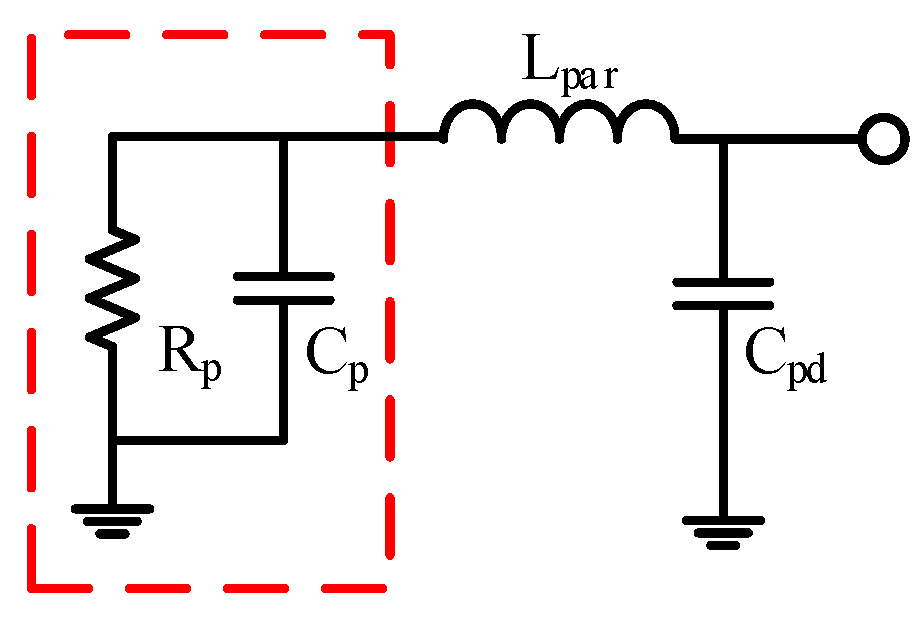
The large-signal output impedance of the active devices can be equivalent to a parallel RC model, as shown in Figure 1. According to the load line theory, the power point Rp is estimated as Equation (1) [8]. In this GaN process, the maximum current Imax and the knee voltage Vknee are 0.8 A/mm and 5 V, respectively. Table 1 shows that the parameters of 0.25 μm GaN HEMT process. The theoretical power point Rp value is about 58 Ω·mm at 28 V operating voltage.
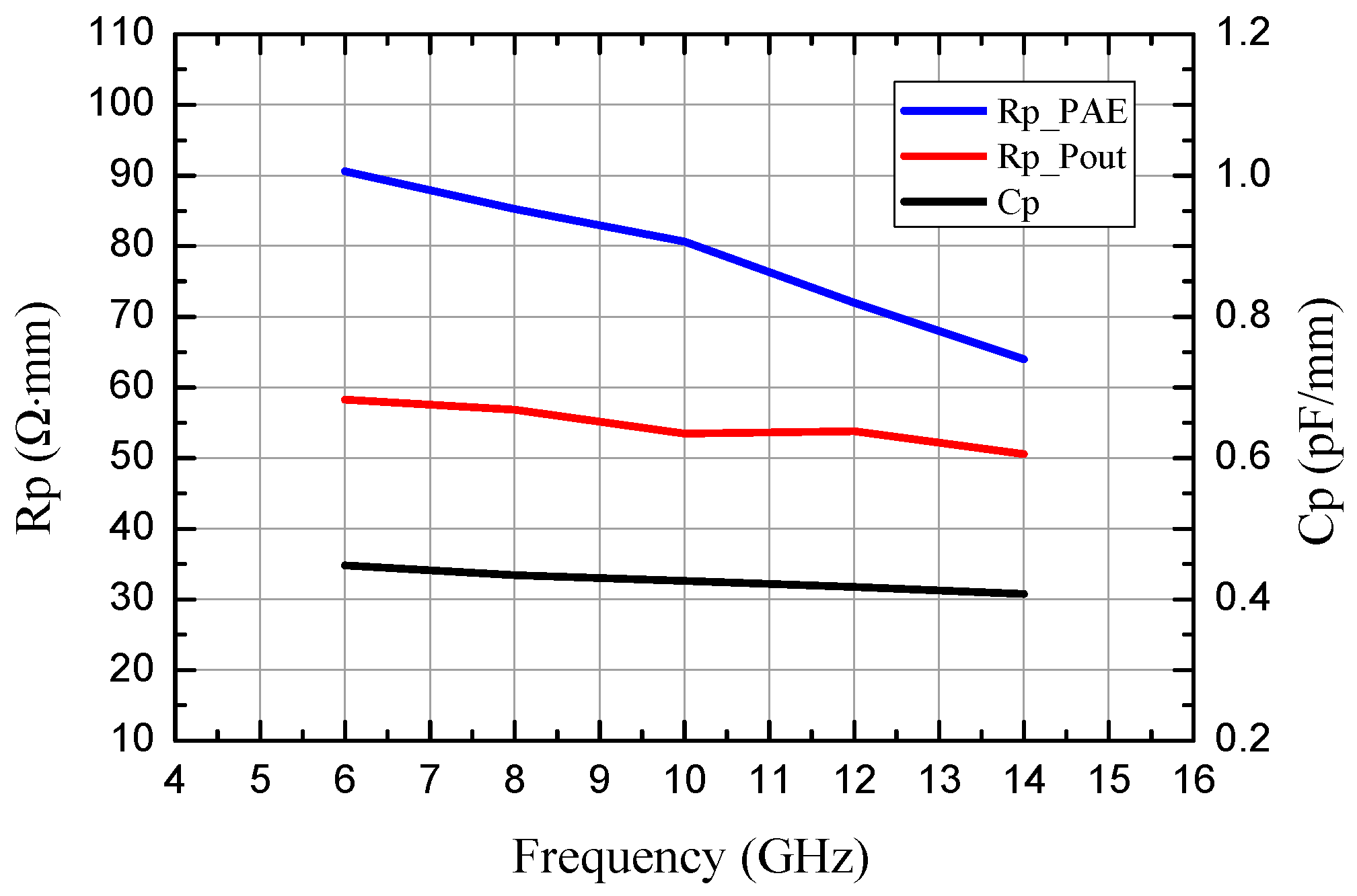
The Cp is mainly composed of the output equivalent capacitance Cds and Cgd, as in Equation (2). Where Ku is the voltage gain. The capacitance Cds and Cgd are 0.3 pF/mm and 0.1 pF/mm, respectively. The optimal Cp value of the efficiency and power are close, and the value is about 0.4 pF/mm. To verify the accuracy of the RC model, we conducted load-pull and S-parameters measurements. The RC values of the large-signal output impedance are extracted through the load-pull and S-parameters measurement data of the GaN HEMTs, as shown in Figure 2. The admittance Y of looking into the device is given by Equation (3).
where Z is the load pull impedance. The RC extraction formulas are shown Equations (4) and (5).
where W is the total gate periphery and ω is the angular frequency. The Rp tends to decrease with increasing frequency. Based on the above theory, the RC model is compared with the measured and the GaN HEMT PDK model data, as shown in Figure 3. For large-signal output impedance, the RC model has higher accuracy than the GaN HEMT PDK model provided by the factory. In addition, the RC model supports the accurate extraction of the large-signal output impedances of GaN HEMTs with arbitrary dimensions. Therefore, in the following design of the broadband impedance matching networks of a GaN HEMT power amplifier MMIC, the RC model is directly used to replace the PDK model as the large-signal output impedance of the GaN HEMT.
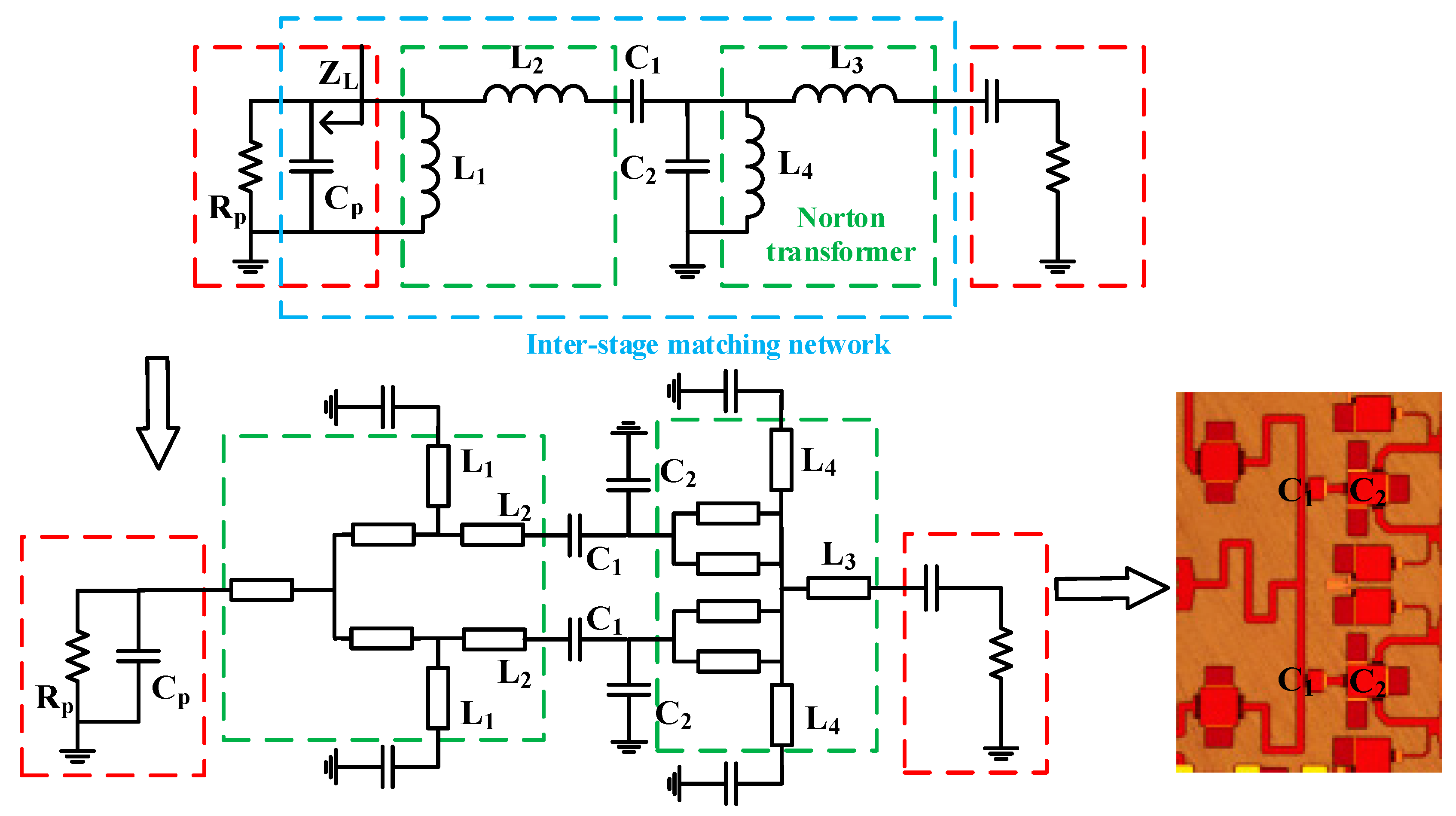
3. Circuit Design
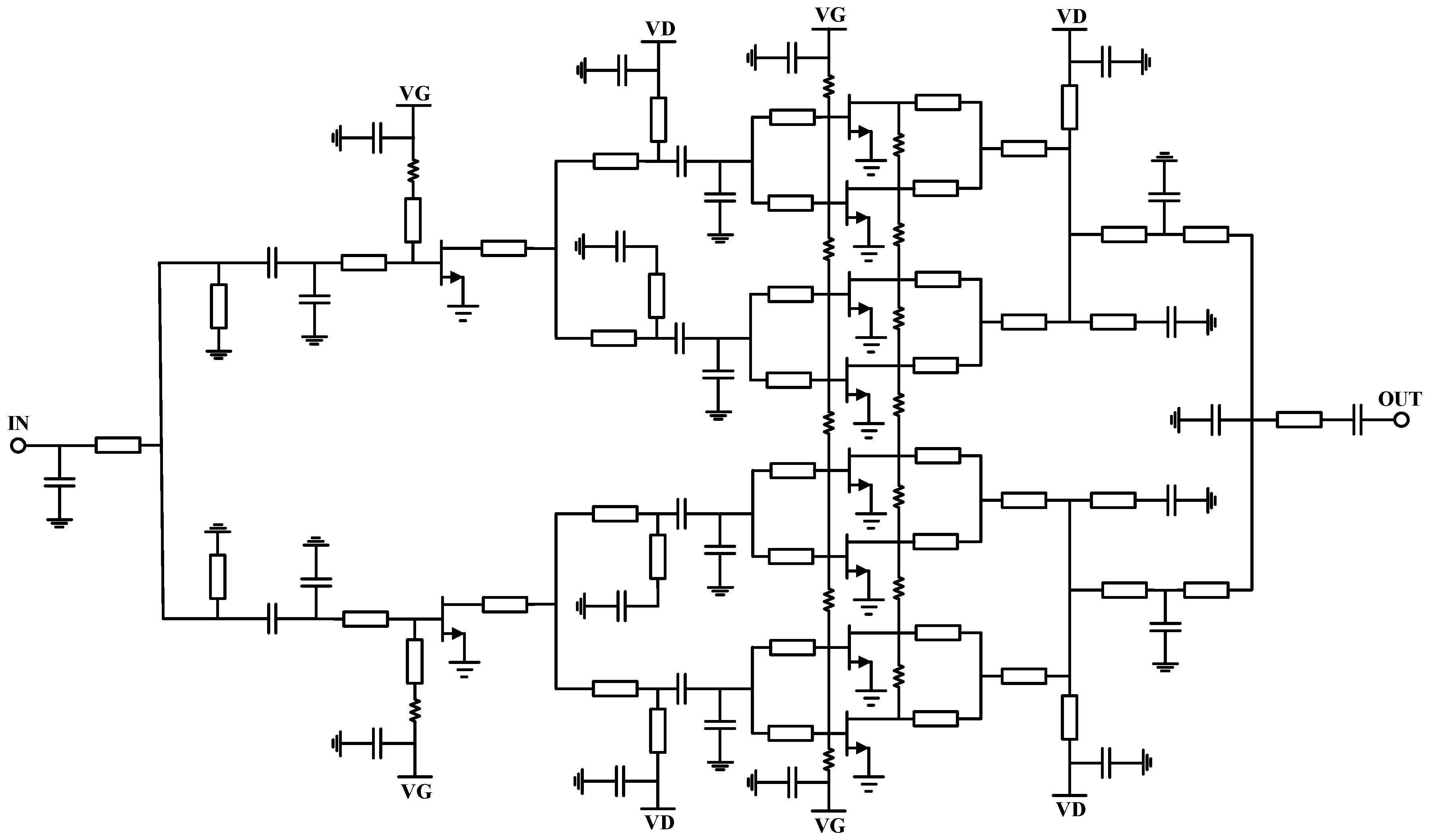
The circuit topology of the proposed power amplifier is shown in Figure 4. The circuit design consists of two stages. The first stage and the second stage use the same HEMT of 8 × 150 μm total gate periphery, and the periphery ratio is 1:4. The RC values of the 8 × 150 μm GaN HEMT are about 70 Ω and 0.45 pF, respectively.
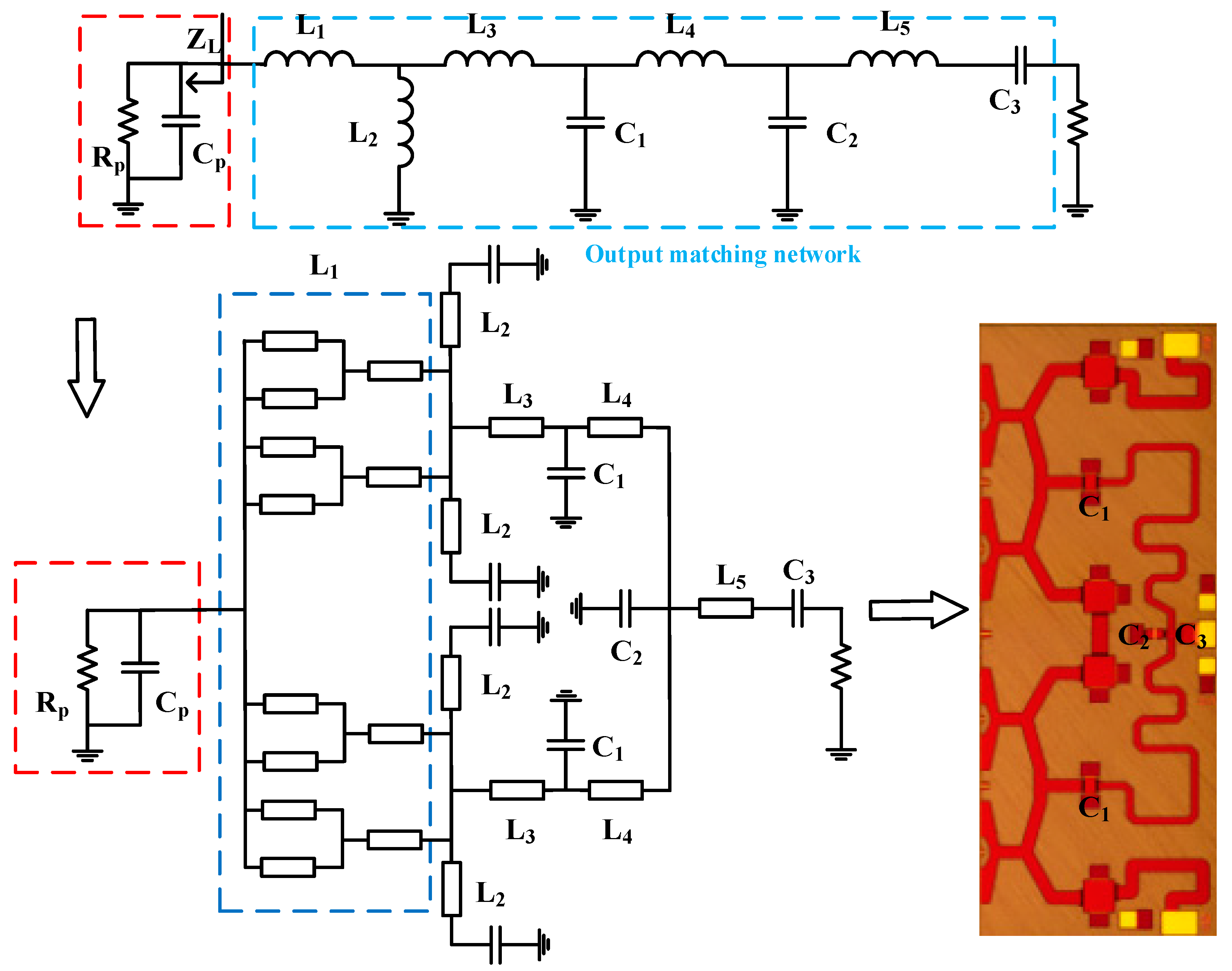
The L-R-C networks are used to guarantee the overall stability of the power amplifier and reduce the Q factor of the matching network. The gain response of the GaN HEMT decreases as the frequency increases, thus the L-R-C networks were designed to provide the compensation of gain flatness. The output matching network is designed to transfer to 50 ohm to equivalent parallel RC model, as shown in Figure 5. To achieve the maximum output power, the output matching network utilizes the band-pass filter topology to reduce the insertion loss. The inter-stage matching network is achieved by using band-pass filter topology to extend the bandwidth [9], as shown in Figure 6. In addition, the equivalent impedance is usually obtained by the Norton transformer network. In the second stage, the resistors are used between each GaN HEMT in order to prevent odd mode oscillation.
4. Measurement Results
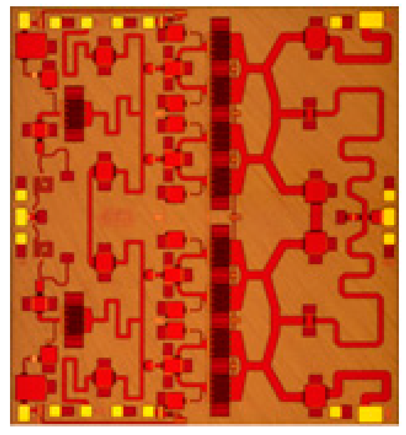
The proposed power amplifier chip photograph is shown in Figure 7, and the total chip size is 3.20 mm × 3.45 mm. The drain and gate voltage bias of the power amplifier are 28 V and −2 V, respectively. The power amplifier measurements are performed under pulsed conditions with 100 μs pulse width and 10% duty cycle.
The average saturated output power is over 40 W from 8 GHz to 12 GHz with 24 dBm input power, as shown in Figure 8a. The associated average power-added efficiency is over 44.7% and the peak power-added efficiency is 51.4% at 8.1 GHz. The small signal gain varies in the range of 24.5 dB to 28 dB and the input reflection coefficient stays below −12.7 dB, as shown in Figure 8b. The measured output power, gain and PAE of the power amplifier versus the input power at 8.8 GHz are shown in Figure 8c. With 26 dBm input power, this power amplifier achieved 52 W output power and 50% power-added efficiency at 8.8 GHz. The measured output power, gain and PAE of the power amplifier versus the input power at 10.4 GHz are shown in Figure 8d. With 26 dBm input power, this power amplifier achieved 43 W output power and 44.5% power-added efficiency at 10.4 GHz. Table 2 summarizes the performance comparison of this power amplifier with the previous published power amplifiers at close frequency ranges. The characteristics of the proposed power amplifier includes power, power-added efficiency, power gain, and size.
5. Conclusions
In this paper, the design of a broadband 40 W power amplifier MMIC over a bandwidth from 8 GHz to 12 GHz is reported. An equivalent RC model is presented which can accurately extract the output impedance of GaN HEMTs and can be used to achieve the broadband matching networks of the power amplifier. The band-pass filter topology is employed to achieve the maximum output power and extend the bandwidth. The measurement results show that this power amplifier has excellent performance with over 40 W output power and 44.7% power-added efficiency at operation frequency.
Author Contributions
Methodology, R.C.; software, S.C.; validation, R.L.; data curation, S.Z.; writing—original draft preparation, R.C.; writing—review and editing, J.H.; supervision, Z.W.; project administration, J.H.; funding acquisition, Z.W.
Funding
This research was funded by the National Natural Science Foundation of China grant number 61604128 and the Fundamental Research Funds for the Central Universities grant number 2017QN81002.
Acknowledgments
The authors would like to thank the Institute of Aerospace Electronics Engineering of Zhejiang University for providing research platform and technical support.
Conflicts of Interest
The authors declare no conflict of interest.
References
- Lee, S.; Park, H.; Choi, K.; Kwon, Y. A Broadband GaN pHEMT Power Amplifier Using Non-Foster Matching. IEEE Trans. Microw. Theory Tech. 2015, 63, 4406–4414. [Google Scholar] [CrossRef]
- Couturier, A.M.; Poitrenaud, N.; Serru, V.; Dionisio, R.; Fontecave, J.J.; Camiade, M. 50% High Efficiency X-Band GaN MMIC Amplifier for Space Applications. In Proceedings of the European Microwave Conference, Madrid, Spain, 23–27 September 2018. [Google Scholar]
- Kuhn, J.; Raay, F.V.; Quay, R.; Kiefer, R.; Peschel, D.; Mikulla, M.; Eggebert, M.S.; Bronner, W.; Schlechtweg, M.; Ambacher, O.; et al. Design of X-Band GaN MMICs Using Field Plates. In Proceedings of the 4th European Microwave Integrated Circuits Conference, Rome, Italy, 28–29 September 2009. [Google Scholar]
- Kuhn, J.; Raay, F.V.; Quay, R.; Kiefer, R.; Maier, T.; Stibal, R.; Mikulla, M.; Eggebert, M.S.; Bronner, W.; Schlechtweg, M.; et al. Design of Highly-Efficient GaN X-Band-Power-Amplifier MMICs. In Proceedings of the IEEE/MTT-S International Microwave Symposium (IMS), Boston, MA, USA, 7–12 June 2009. [Google Scholar]
- Wohlmuth, W.; Weng, M.H.; Lin, C.K.; Du, J.H.; Ho, S.Y.; Chou, T.Y.; Li, S.M.; Huang, C.; Wang, W.C.; Wang, W.K. AlGaN/GaN HEMT Development Targeted for X-band Applications. In Proceedings of the IEEE International Conference on Microwaves, Communications, Antennas and Electronic Systems (COMCAS), Tel Aviv, Israel, 21–23 October 2013. [Google Scholar]
- Schuh, P.; Sledzik, H.; Reber, R.; Fleckenstein, A.; Leberer, R.; Oppermann, M.; Quay, R.; Raay, F.V.; Eggebert, M.S.; Kiefer, R.; et al. GaN MMIC based T/R-Module Front-End for X-band Applications. In Proceedings of the 3rd European Microwave Integrated Circuits Conference, Amsterdam, The Netherlands, 27–28 October 2008. [Google Scholar]
- Chu, C.K.; Huang, H.K.; Liu, H.Z.; Lin, C.H.; Chang, C.H.; Wu, C.L.; Chang, C.S.; Wang, Y.H. An X-Band High-Power and High-PAE PHEMT MMIC Power Amplifier for Pulse and CW Operation. IEEE Microw. Wirel. Compon. Lett. 2008, 18, 707–709. [Google Scholar] [CrossRef]
- Formicone, G.; Burger, J.; Custer, J.; Keshishian, R.; Veitschegger, W. A Study for Achieving High Power and Efficiency based on High Bias Operation in C- and X-band GaN Power Amplifiers. In Proceedings of the IEEE Topical Conference on RF/Microwave Power Amplifiers for Radio and Wireless Applications (PAWR), Anaheim, CA, USA, 14–17 January 2018. [Google Scholar]
- Meng, X.Y.; Yu, C.P.; Liu, Y.N.; Wu, Y.L. Design Approach for Implementation of Class-J Broadband Power Amplifiers Using Synthesized Band-Pass and Low-Pass Matching Topology. IEEE Trans. Microw. Theory Tech. 2017, 65, 4984–4996. [Google Scholar]
- Bent, G.V.D.; Hek, A.P.D.; Bessemoulin, A.; Vliet, F.E.V. Low-Cost High-Efficient 10-Watt X-band High-Power Amplifier. In Proceedings of the IEEE International Conference on Microwaves, Communications, Antennas and Electronics Systems, Tel Aviv, Israel, 9–11 November 2009. [Google Scholar]
- Resca, D.; Raffo, A.; Falco, S.D.; Scappaviva, F.; Vadalà, V.; Vannini, G. X-Band GaN Power Amplifier for Future Generation SAR Systems. IEEE Microw. Wirel. Compon. Lett. 2014, 24, 266–268. [Google Scholar] [CrossRef]
- Costrini, C.; Cetronio, A.; Romanini, P.; Breglio, G.; Irace, A.; Riccio, M. 50W X-band GaN MMIC HPA: Effective Power Capability and Transient Thermal Analysis. In Proceedings of the 5th European Microwave Integrated Circuits Conference, Paris, France, 27–28 September 2010. [Google Scholar]
- Costrini, M.; Calori, M.; Cetronio, A.; Lanzieri, C.; Lavanga, S.; Peroni, M.; Limiti, E.; Serino, A.; Ghione, G.; Melone, G. A 20 Watt Micro-strip X-Band AlGaN/GaN HPA MMIC for Advanced Radar Applications. In Proceedings of the 1st European Wireless Technology Conference, Amsterdam, The Netherlands, 27–28 October 2008. [Google Scholar]
- Piotrowicz, S.; Ouarch, Z.; Chartier, E.; Aubry, R.; Callet, G.; Floriot, D.; Jacquet, J.C.; Jardel, O.; Morvan, E.; Reveyrand, T.; et al. 43W, 52% P AE X-Band AlGaN/GaN HEMTs MMIC Amplifiers. In Proceedings of the IEEE/MTT-S International Microwave Symposium (IMS), Anaheim, CA, USA, 23–28 May 2010. [Google Scholar]
- Shin, D.H.; Yom, I.B.; Kim, D.W. X-Band GaN MMIC Power Amplifier for the SSPA of a SAR System. In Proceedings of the IEEE International Symposium on Radio-Frequency Integration Technology (RFIT), Seoul, Korea, 30 August–1 September 2017. [Google Scholar]
Figure 1.
RC model of active devices’ large-signal output impedance.

Figure 2.
The Rp and Cp parameters versus frequency.

Figure 3.
Comparison of 8–12 GHz optimal efficiency point impedance with measured, RC model, and GaN HEMT PDK model.
Figure 3.
Comparison of 8–12 GHz optimal efficiency point impedance with measured, RC model, and GaN HEMT PDK model.

Figure 4.
The circuit topology of the power amplifier.

Figure 5.
Output matching network.

Figure 6.
Inter-stage matching network.

Figure 7.
Photograph of X-band 40W power amplifier.

Figure 8.
(a) Measured output power, gain, and PAE versus frequency at 24 dBm input power; (b) Measured S-parameter versus frequency; (c) Measured output power, gain, and PAE versus input power at 8.8 GHz frequency; (d) Measured output power, gain, and PAE versus input power at 10.4 GHz frequency.
Figure 8.
(a) Measured output power, gain, and PAE versus frequency at 24 dBm input power; (b) Measured S-parameter versus frequency; (c) Measured output power, gain, and PAE versus input power at 8.8 GHz frequency; (d) Measured output power, gain, and PAE versus input power at 10.4 GHz frequency.


Table 1.
The parameters of 0.25 μm GaN HEMT process.
| Parameter | Value | Parameter | Value |
|---|---|---|---|
| VTH (V) | −2.9 | ft (GHz) | 24.5 |
| VBDG (V) | 121 | fmax (GHz) | 75 |
| Idmax (mA/mm) | 800 | Pdensity (W/mm) | 5 |
| Gm_Peak (mS/mm) | 390 | CMIM (pF/mm2) | 215 |
Table 2.
Performance comparison of relevant power amplifiers.
| Reference | Process | Frequency (GHz) | Pout (W) | PAE (%) | Gp (dB) | Stage | Pulse/Duty (μs, %) | Size (mm2) |
|---|---|---|---|---|---|---|---|---|
| [10] | 0.25 μm GaAs | 8.25–10.25 | 10.7 | 41.4 | 19 | 2 | 3, 3 | 4.41 × 2.5 |
| [11] | 0.25 μm GaN | 8.8–10.4 | 14 | 38 | 18 | 2 | 50, 15 | 4.5 × 4.0 |
| [12] | 0.5 μm GaN | 8–10.5 | 20 | 35 | 15 | 2 | 100, 25 | 5.0 × 3.2 |
| [13] | 0.5 μm GaN | 8.5–9 | 30 | 40 | 14 | 2 | 10, 1 | 5.33 × 3.5 |
| [14] | 0.25 μm GaN | 8.5–10.5 | 35 | 40 | 14 | 2 | 20, 10 | 4.5 × 4.0 |
| [15] | 0.25 μm GaN | 8.8–10.8 | 40 | 44 | 17 | 2 | 100, 10 | 4.5 × 4.6 |
| This work | 0.25 μm GaN | 8–12 | 40 | 44.7 | 22 | 2 | 100, 10 | 3.20 × 3.45 |
© 2019 by the authors. Licensee MDPI, Basel, Switzerland. This article is an open access article distributed under the terms and conditions of the Creative Commons Attribution (CC BY) license (http://creativecommons.org/licenses/by/4.0/).
Share and Cite
MDPI and ACS Style
Chen, R.; Li, R.; Zhou, S.; Chen, S.; Huang, J.; Wang, Z. An X-Band 40 W Power Amplifier GaN MMIC Design by Using Equivalent Output Impedance Model. Electronics 2019, 8, 99. https://doi.org/10.3390/electronics8010099
AMA Style
Chen R, Li R, Zhou S, Chen S, Huang J, Wang Z. An X-Band 40 W Power Amplifier GaN MMIC Design by Using Equivalent Output Impedance Model. Electronics. 2019; 8(1):99. https://doi.org/10.3390/electronics8010099
Chicago/Turabian StyleChen, Ruitao, Ruchun Li, Shouli Zhou, Shi Chen, Jianhua Huang, and Zhiyu Wang. 2019. "An X-Band 40 W Power Amplifier GaN MMIC Design by Using Equivalent Output Impedance Model" Electronics 8, no. 1: 99. https://doi.org/10.3390/electronics8010099
Note that from the first issue of 2016, this journal uses article numbers instead of page numbers. See further details here.