A 10 kW ZVS Integrated Boost Dual Three-Phase Bridge DC–DC Resonant Converter for a Linear Generator-Based Wave-Energy System: Design and Simulation

Abstract
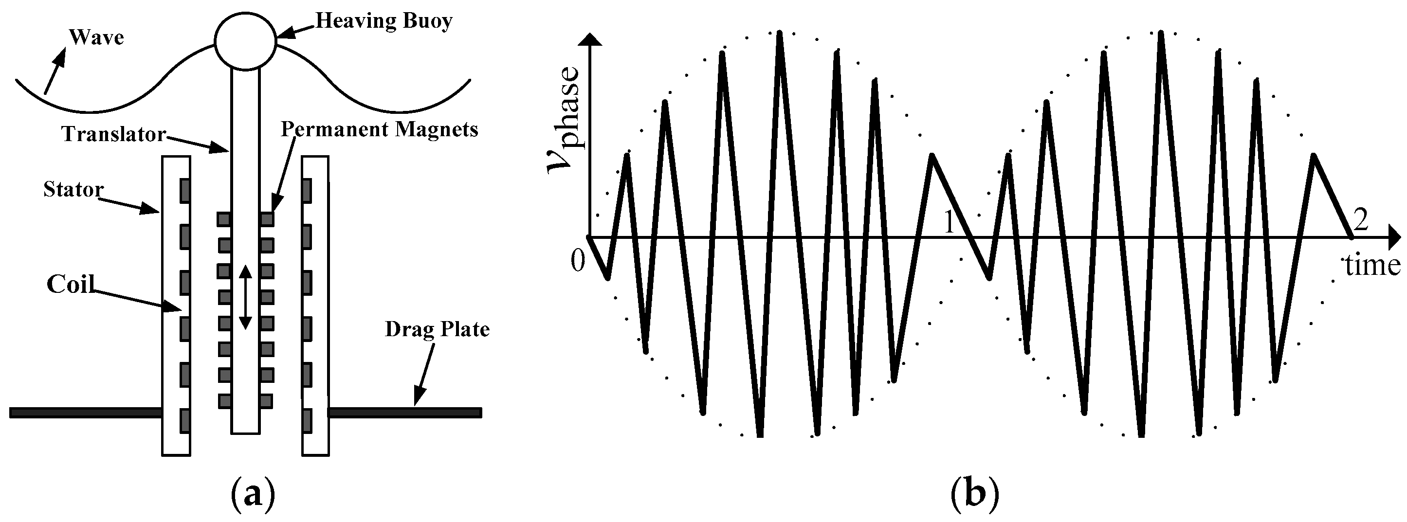
:1. Introduction
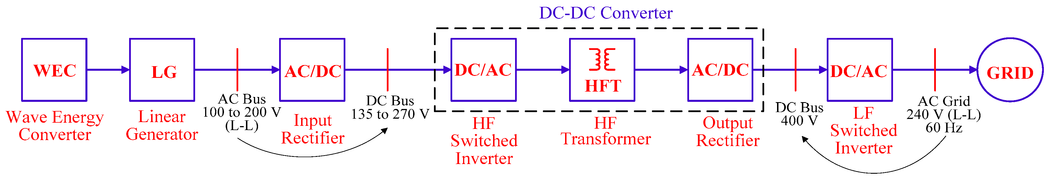
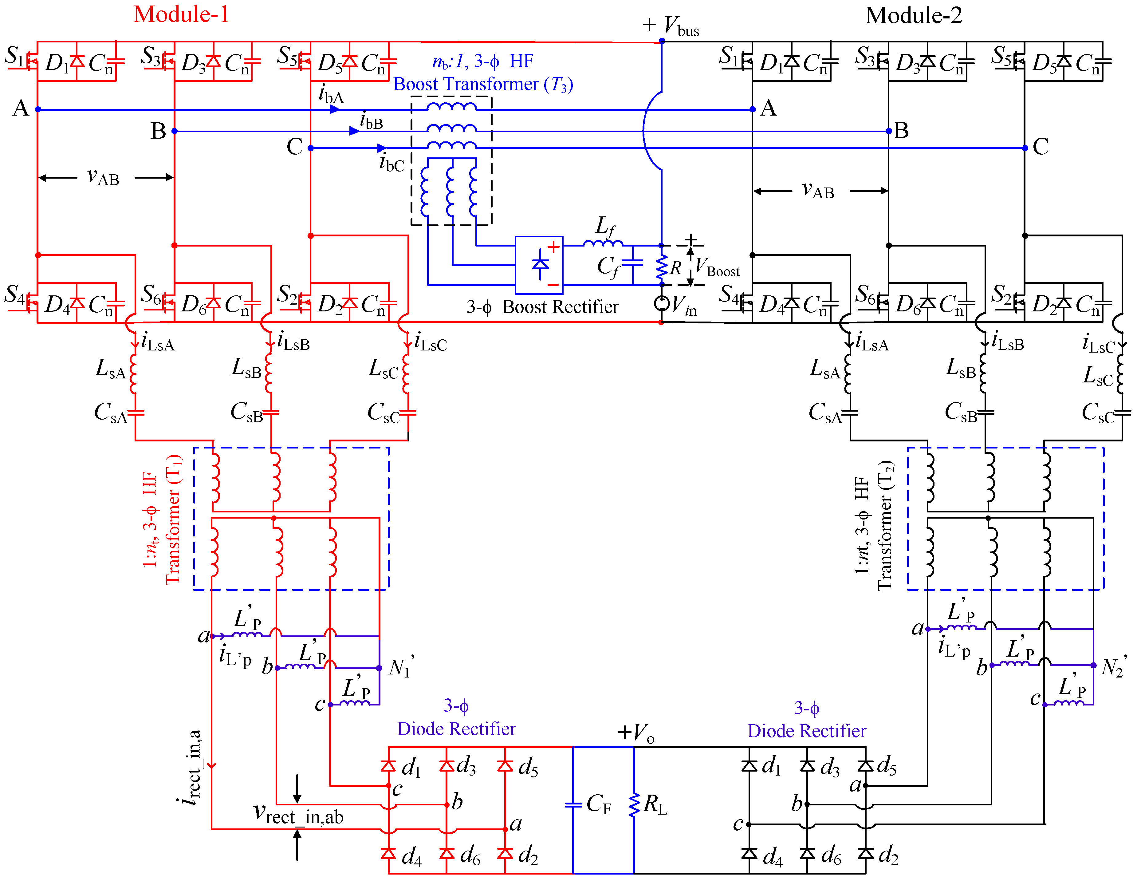
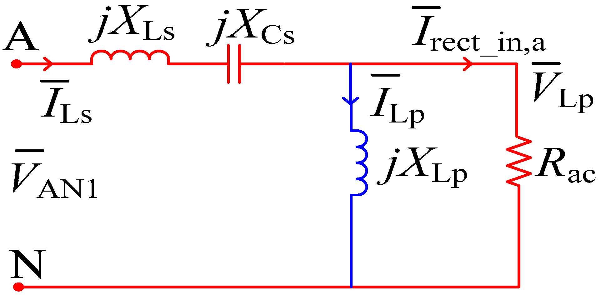
2. Circuit Details of the Designed Converter
3. Design
3.1. Selection of Voltage and Power Ratings
3.2. Design Summary
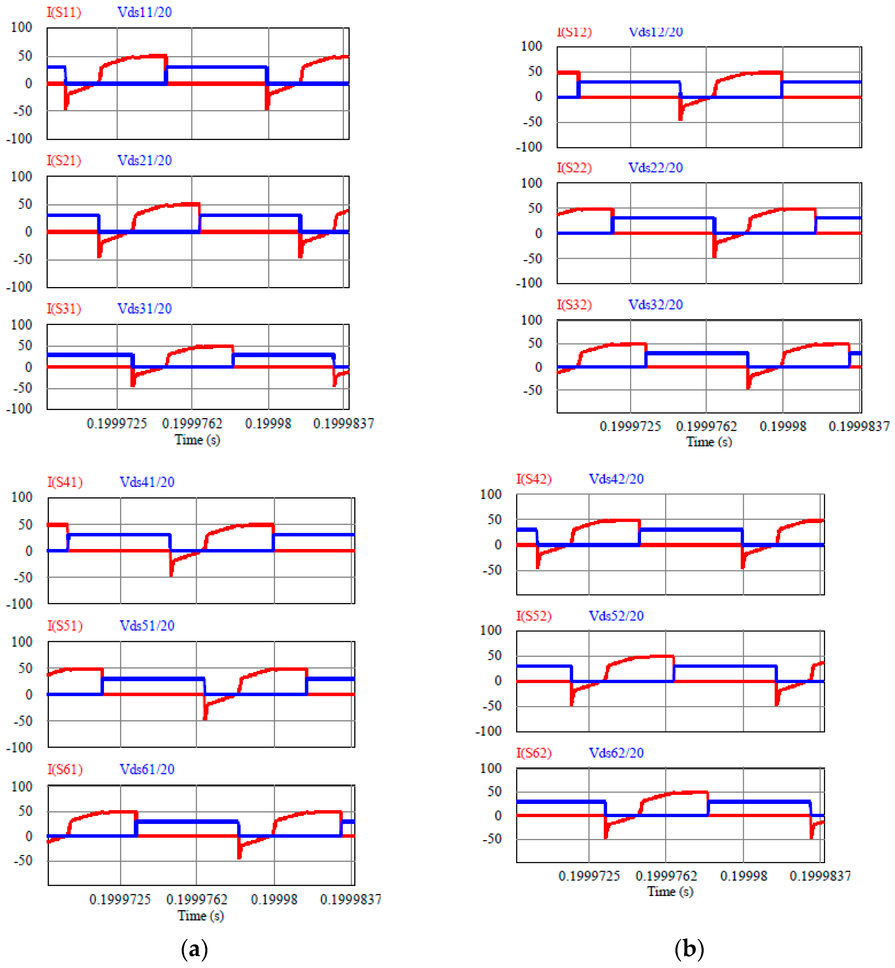
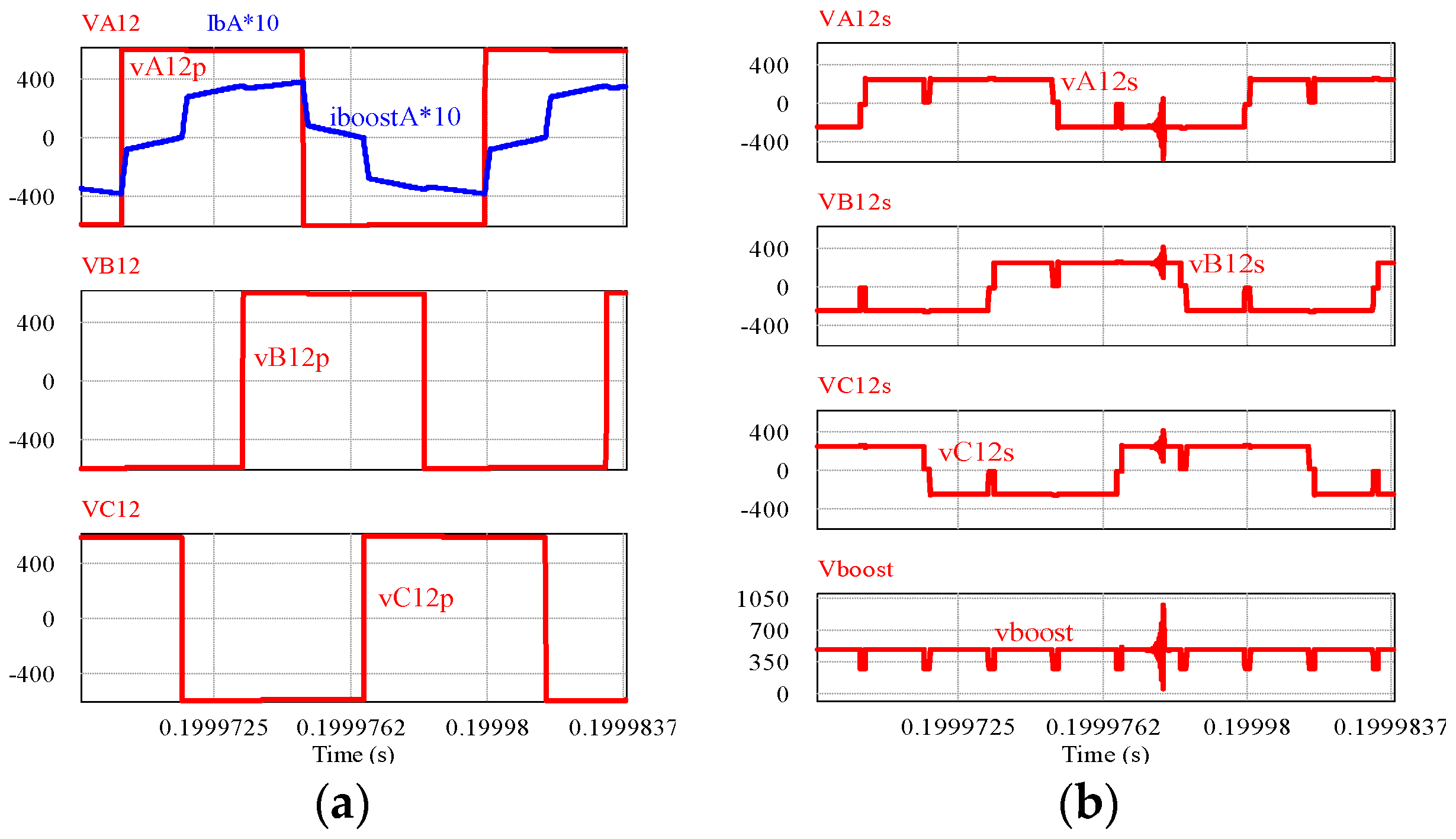
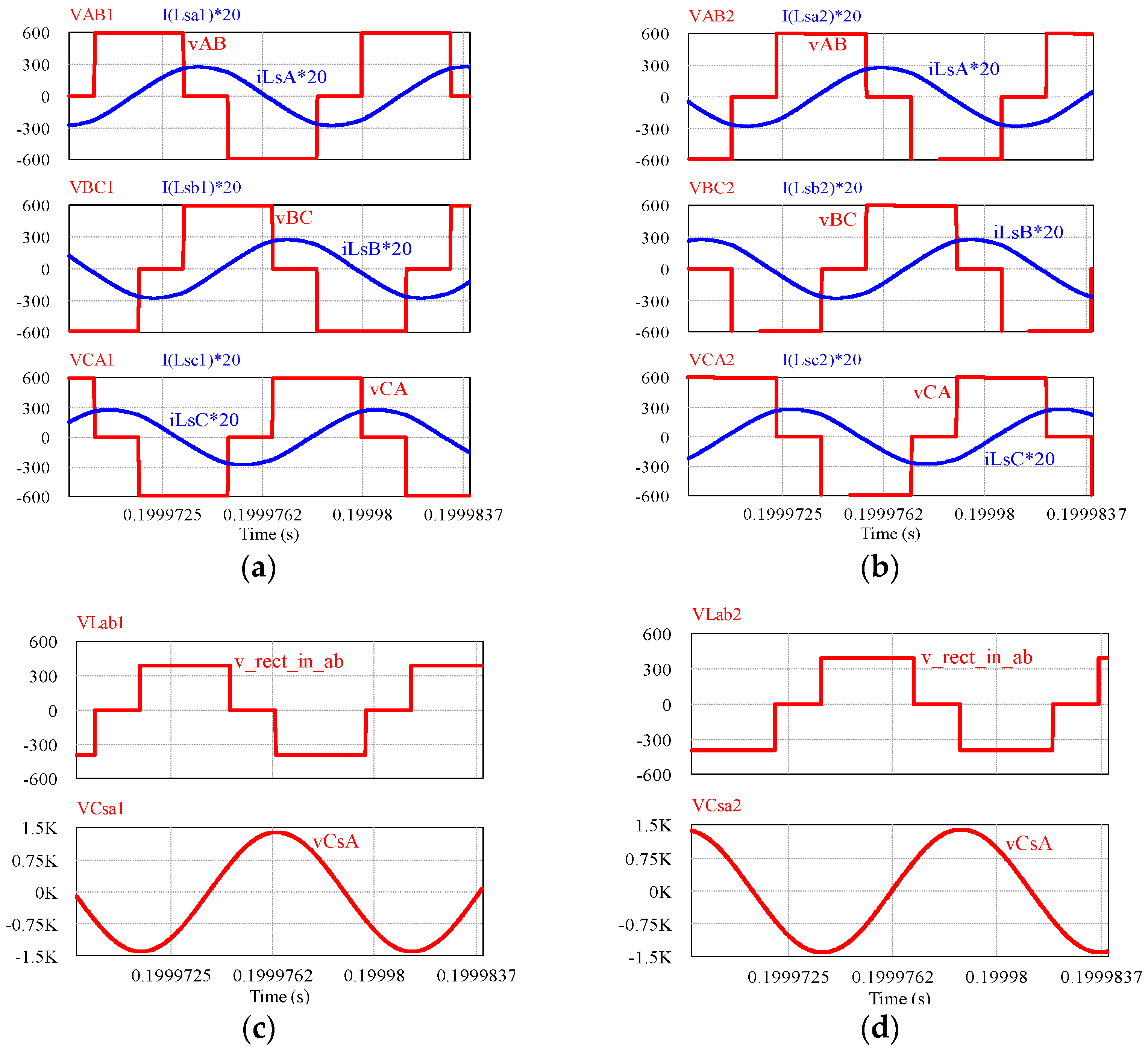
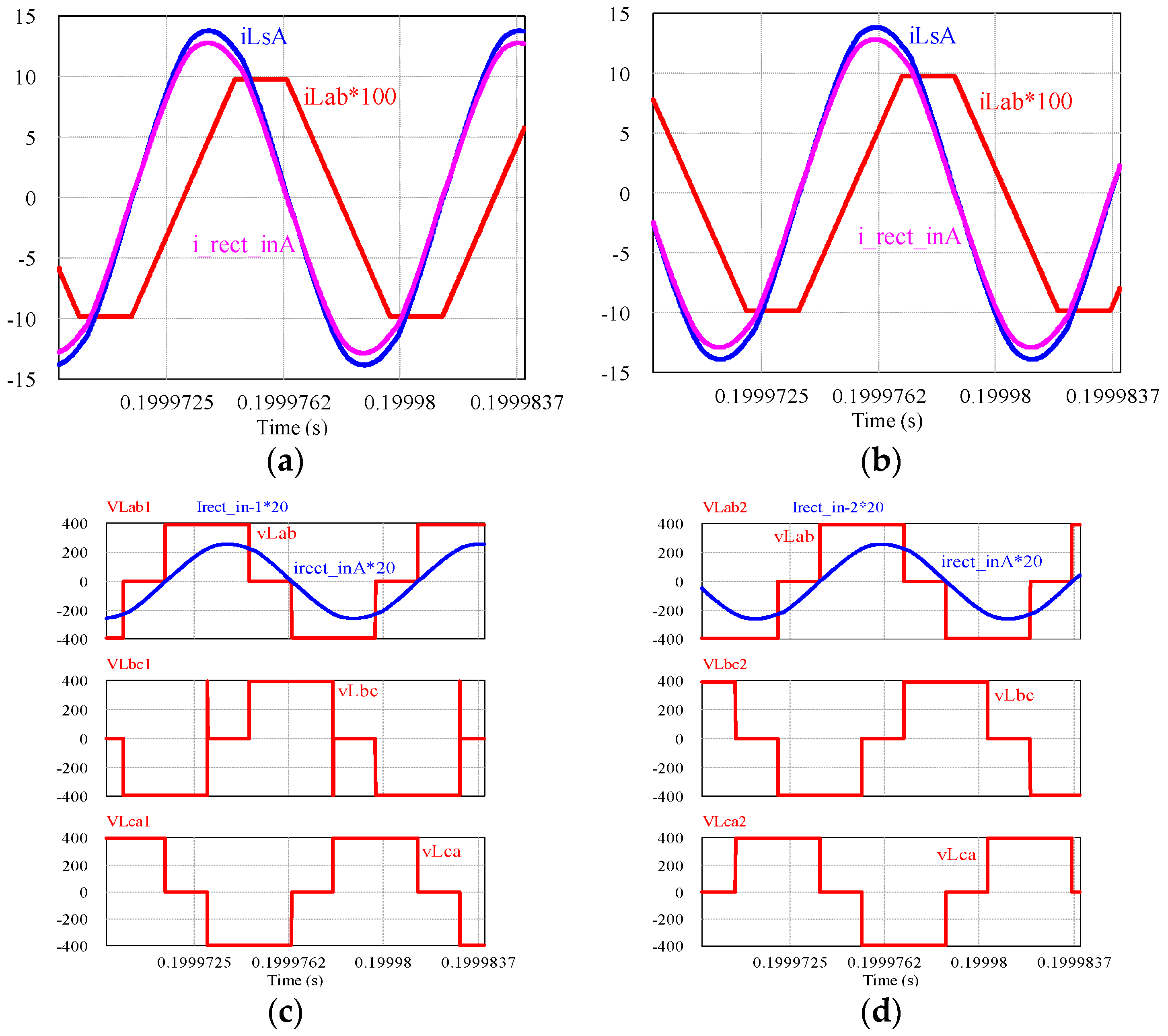
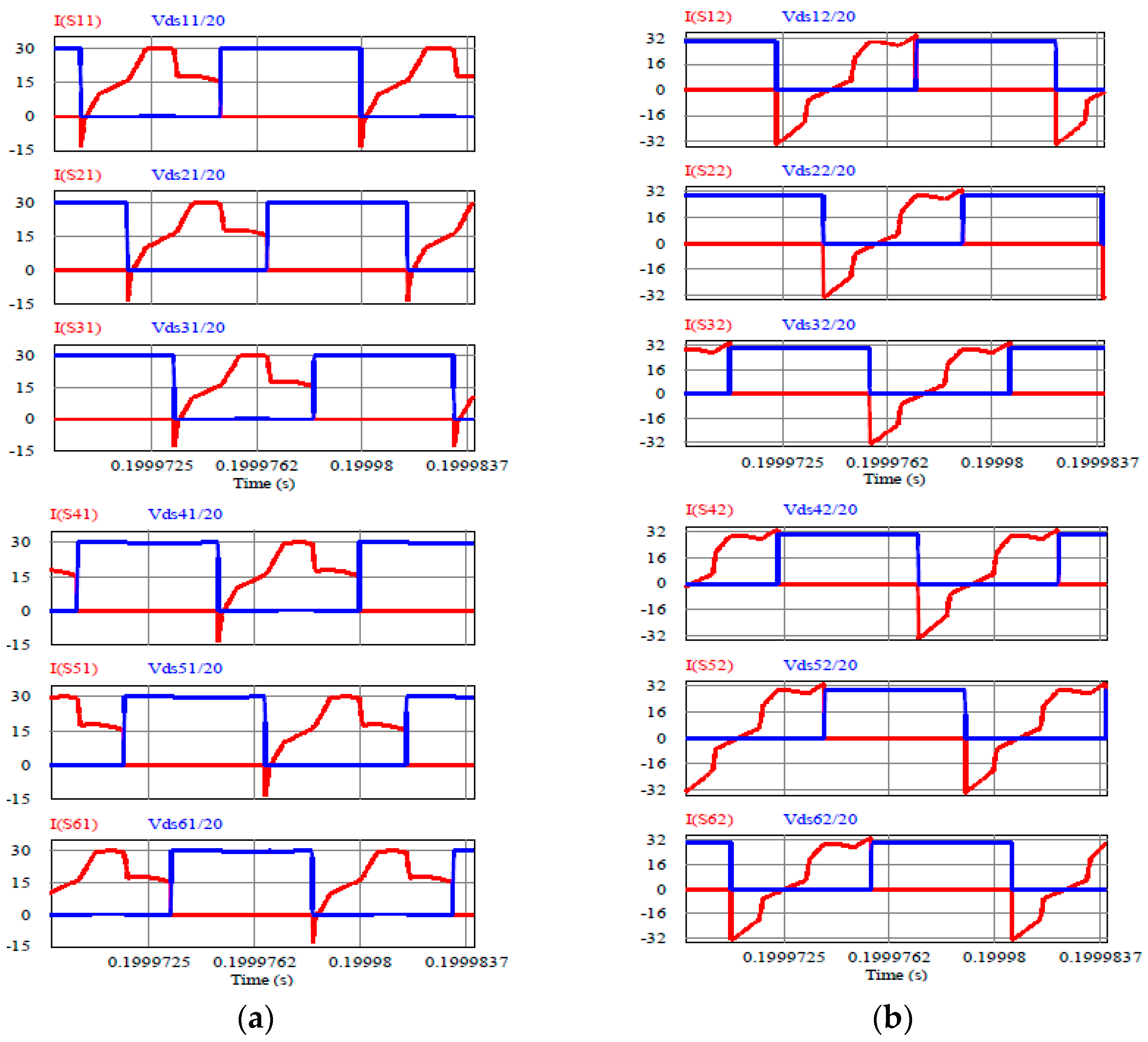
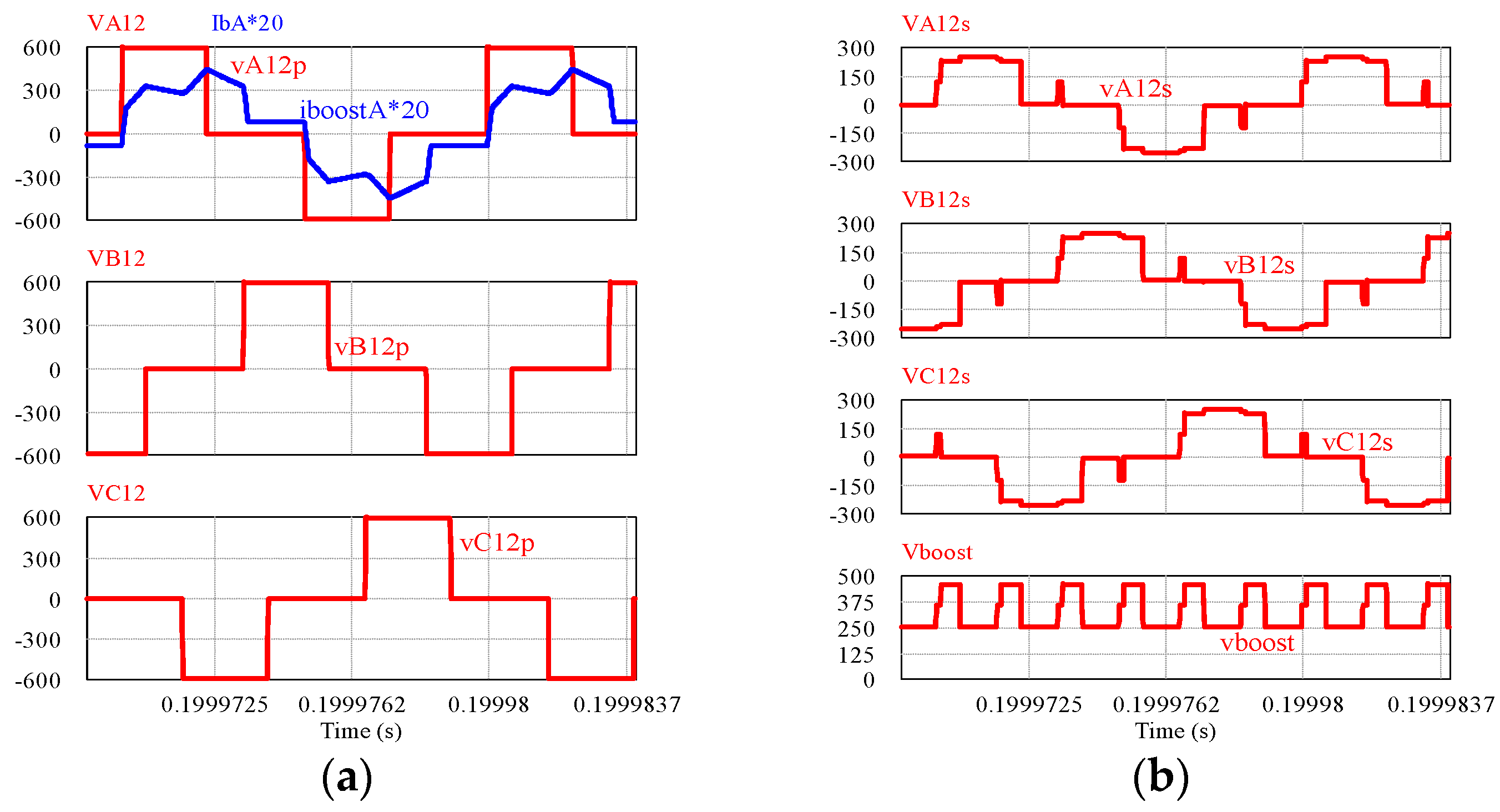
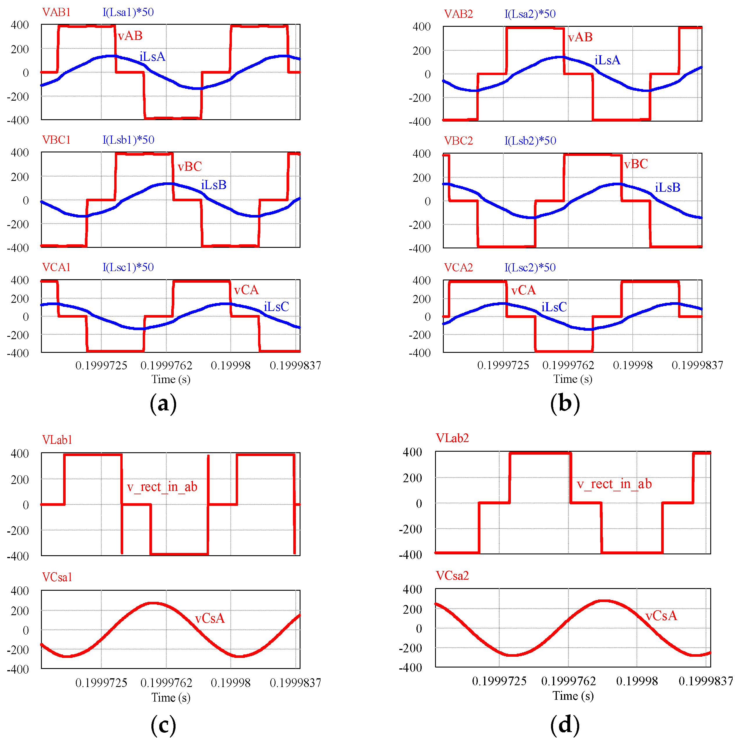
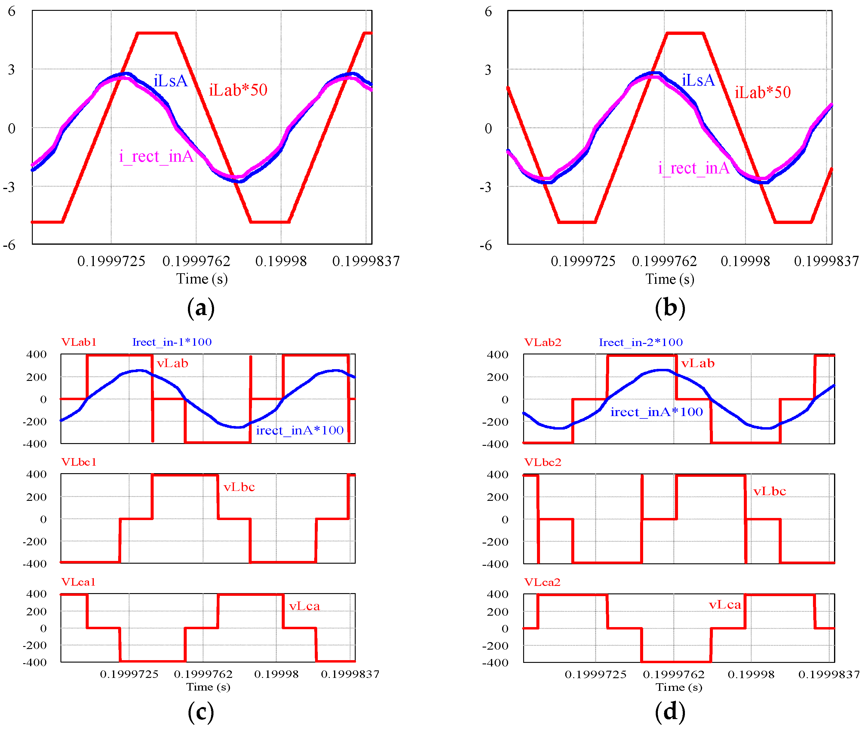
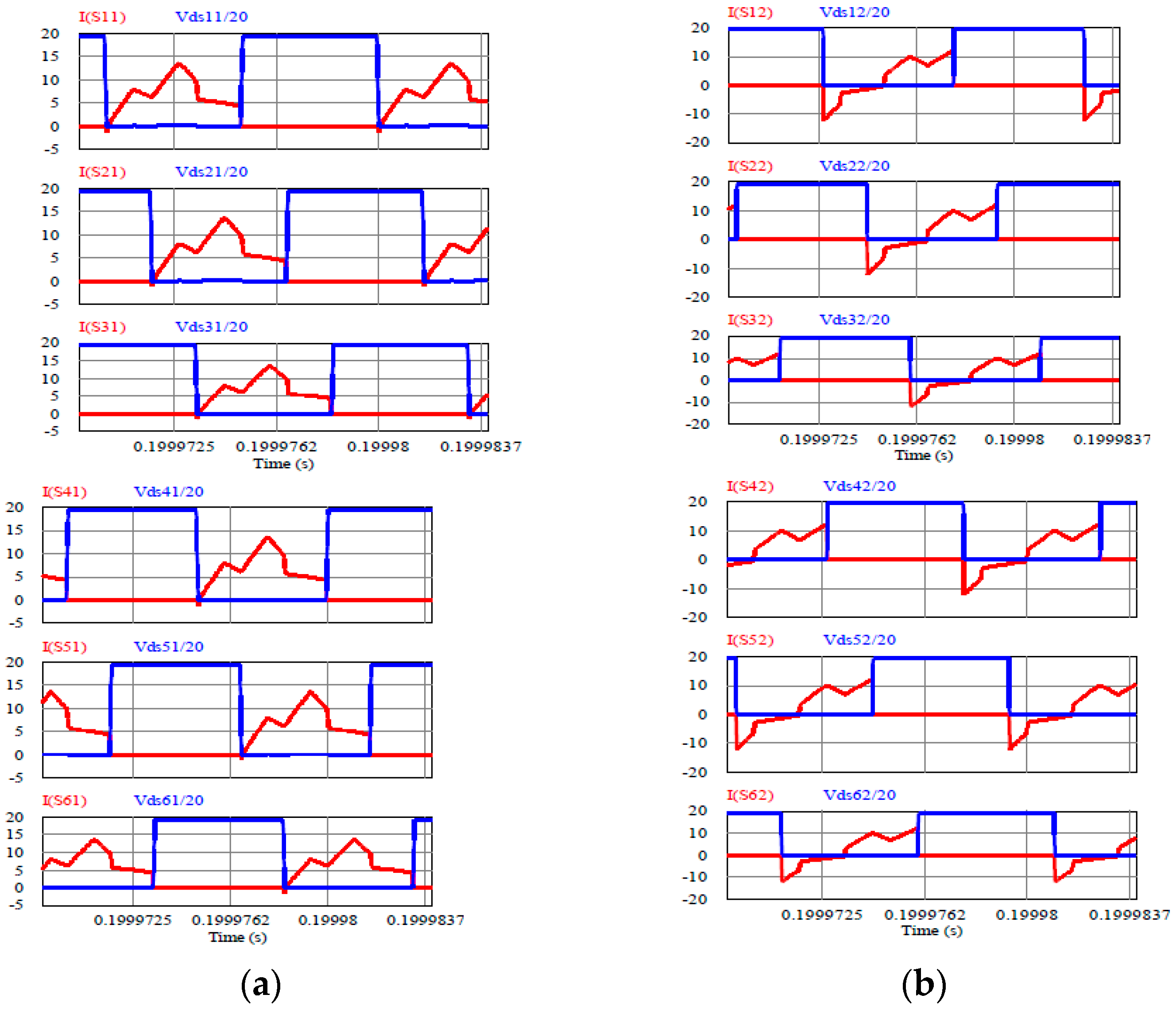
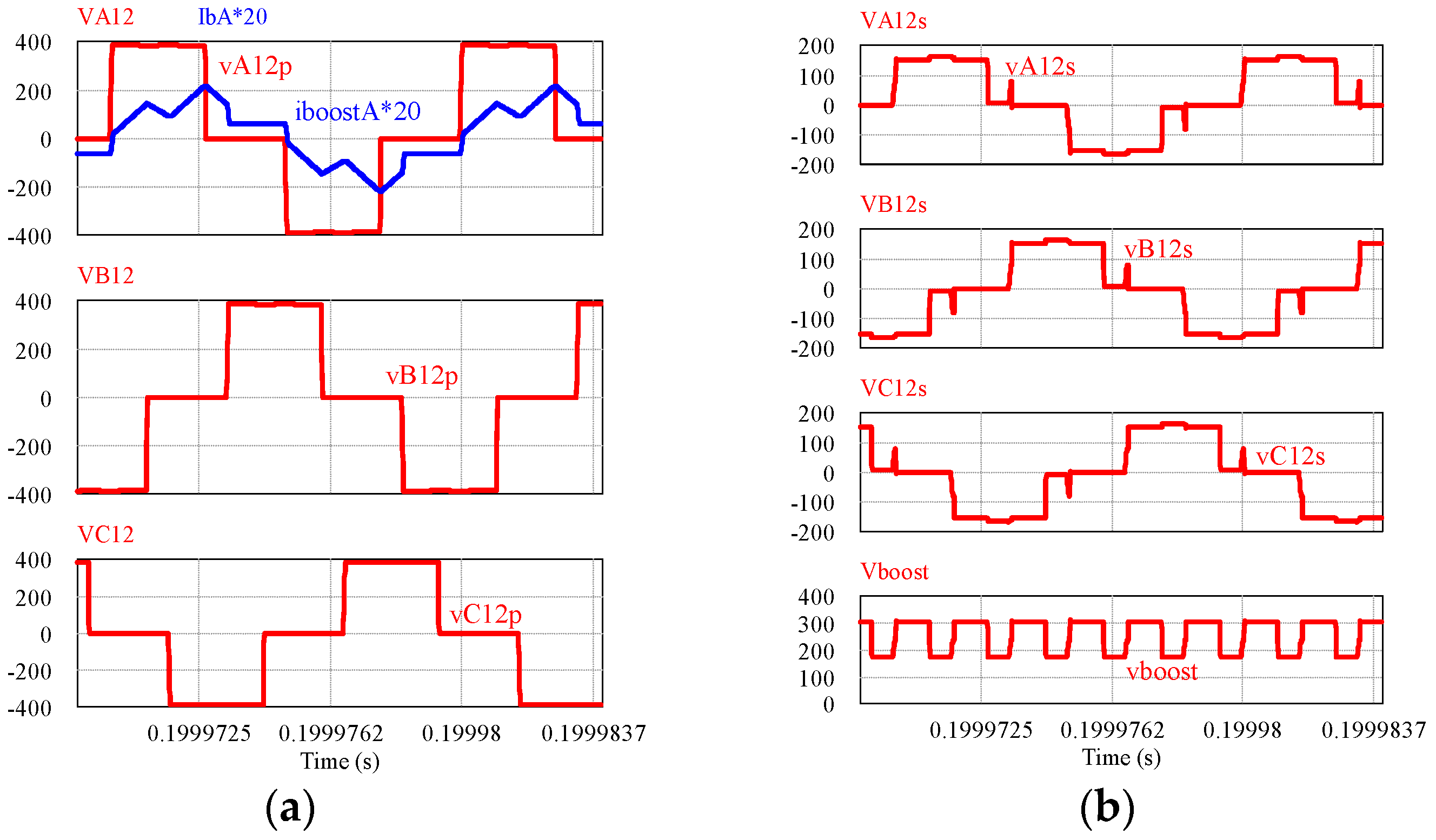
4. Simulation Results
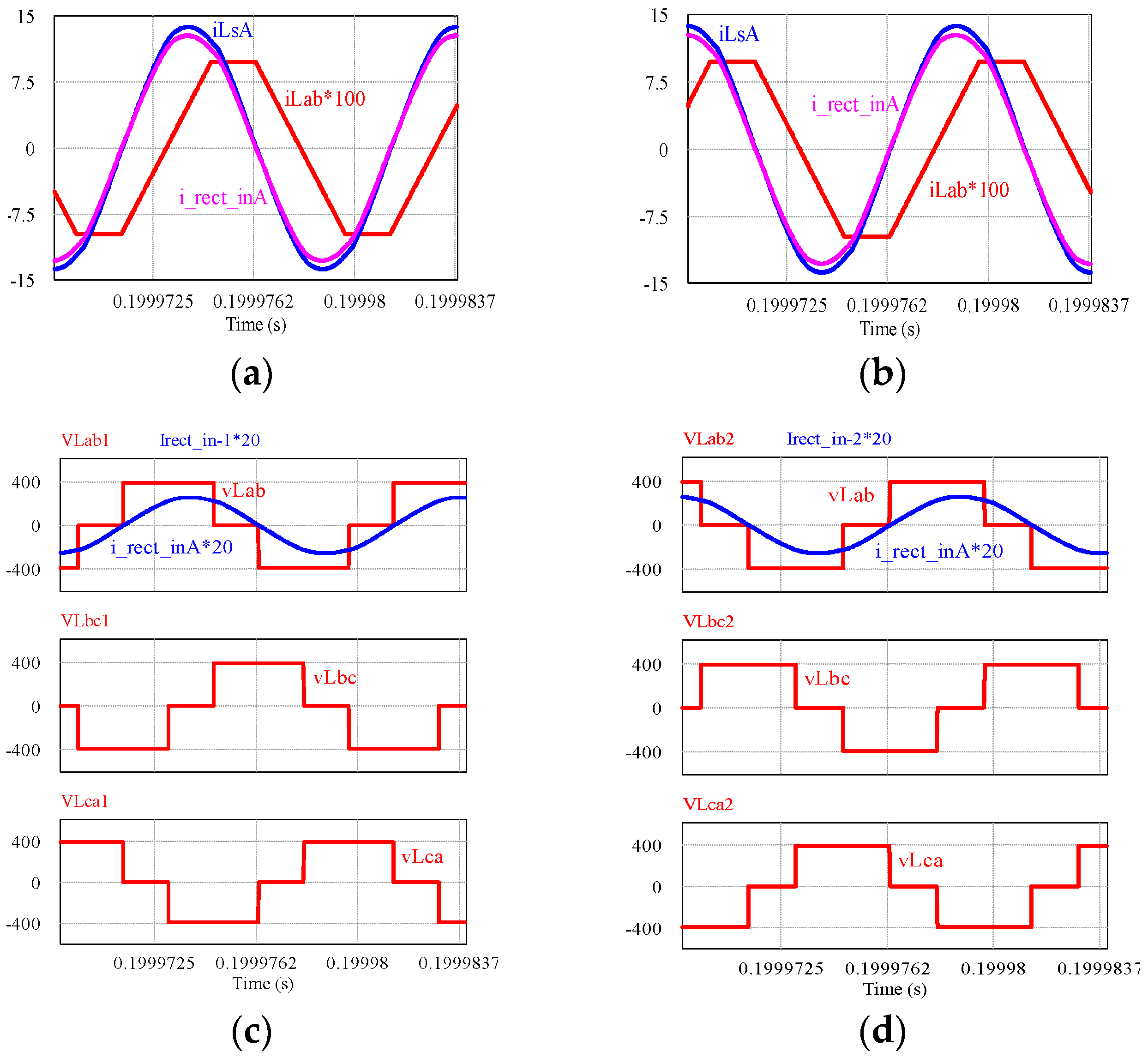
4.1. Steady-State Conditions
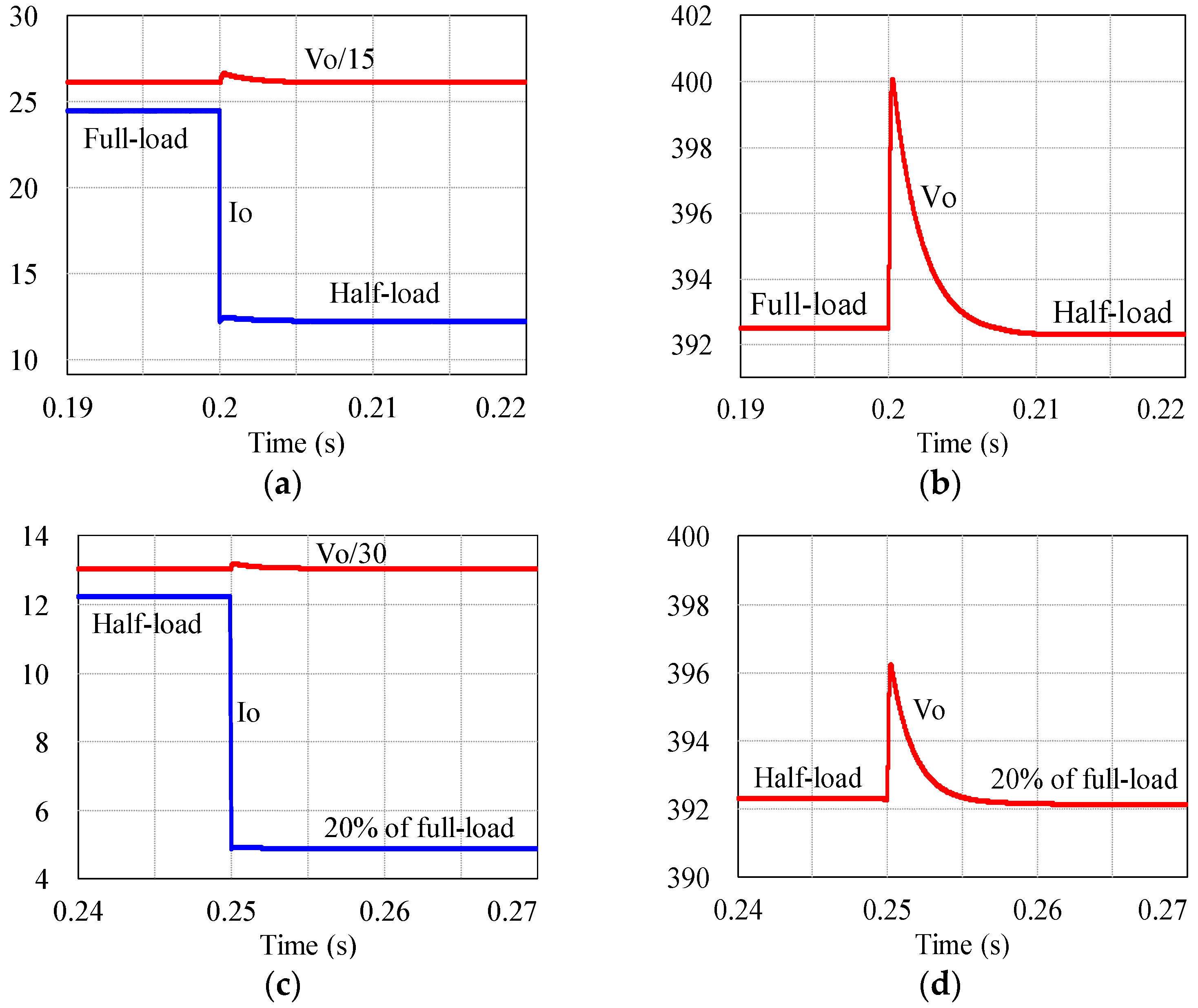
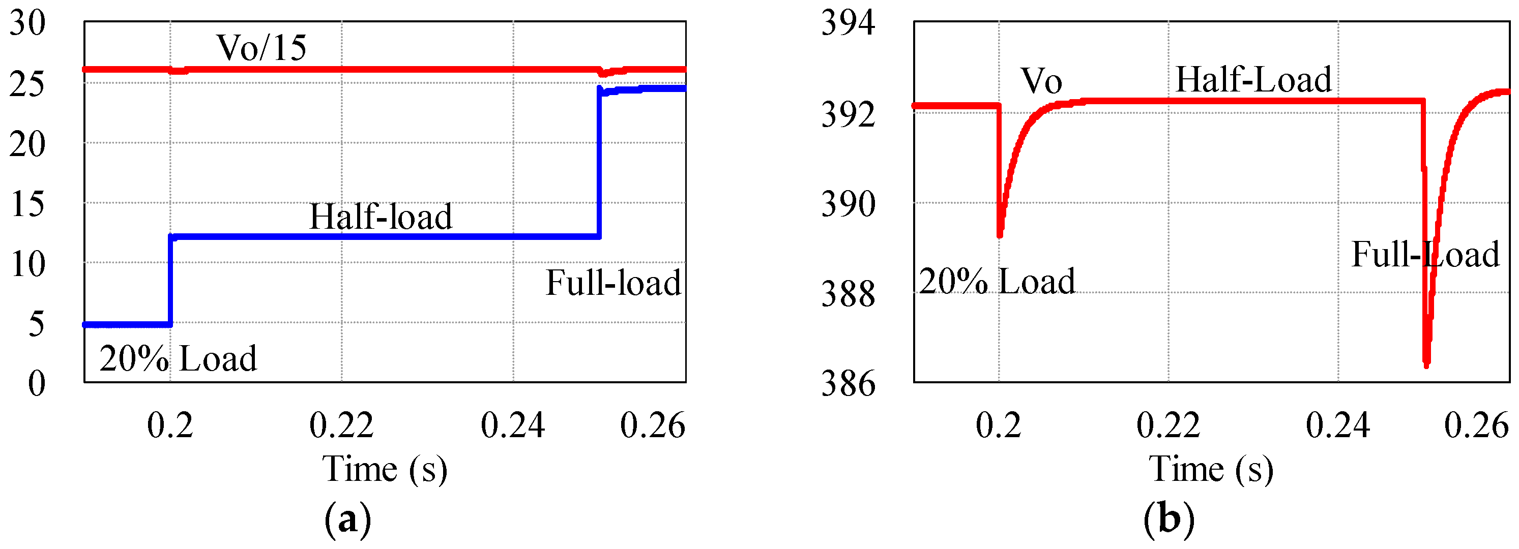
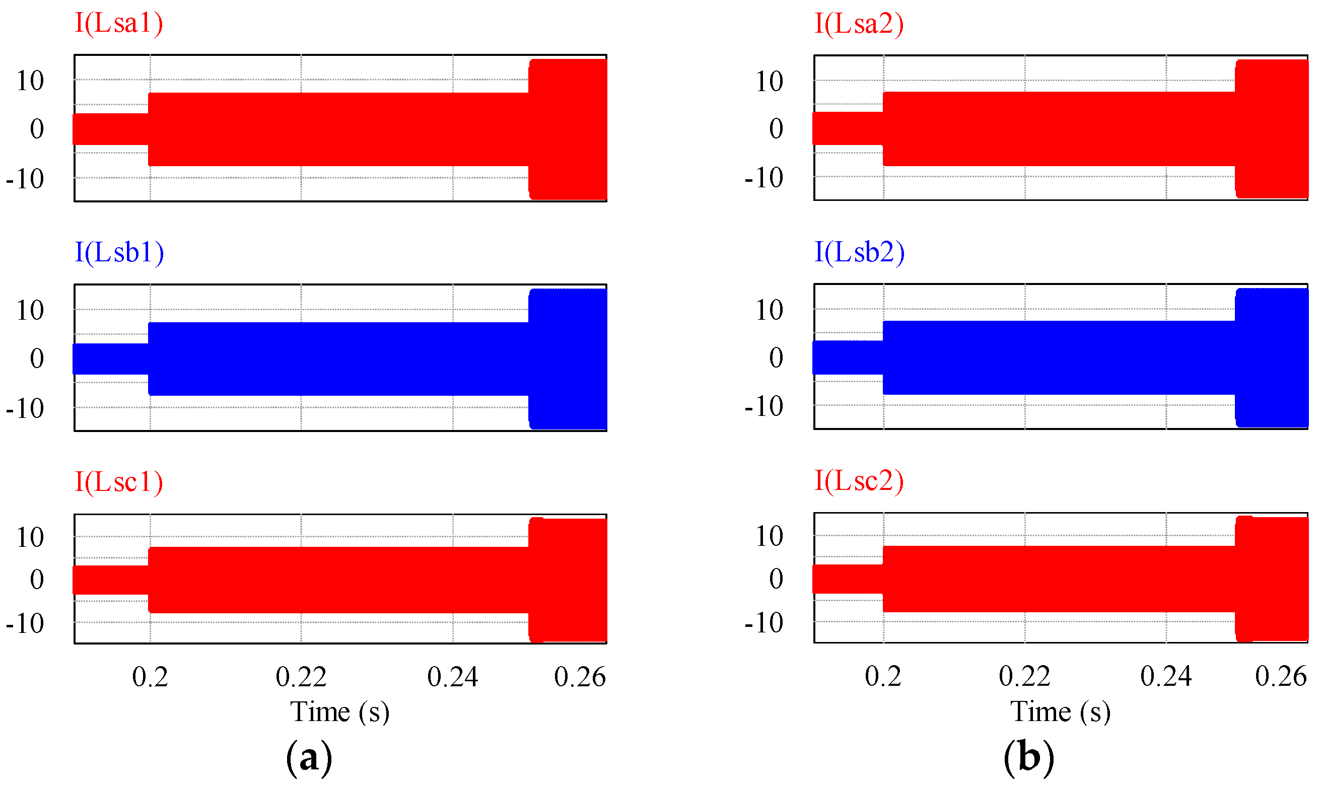
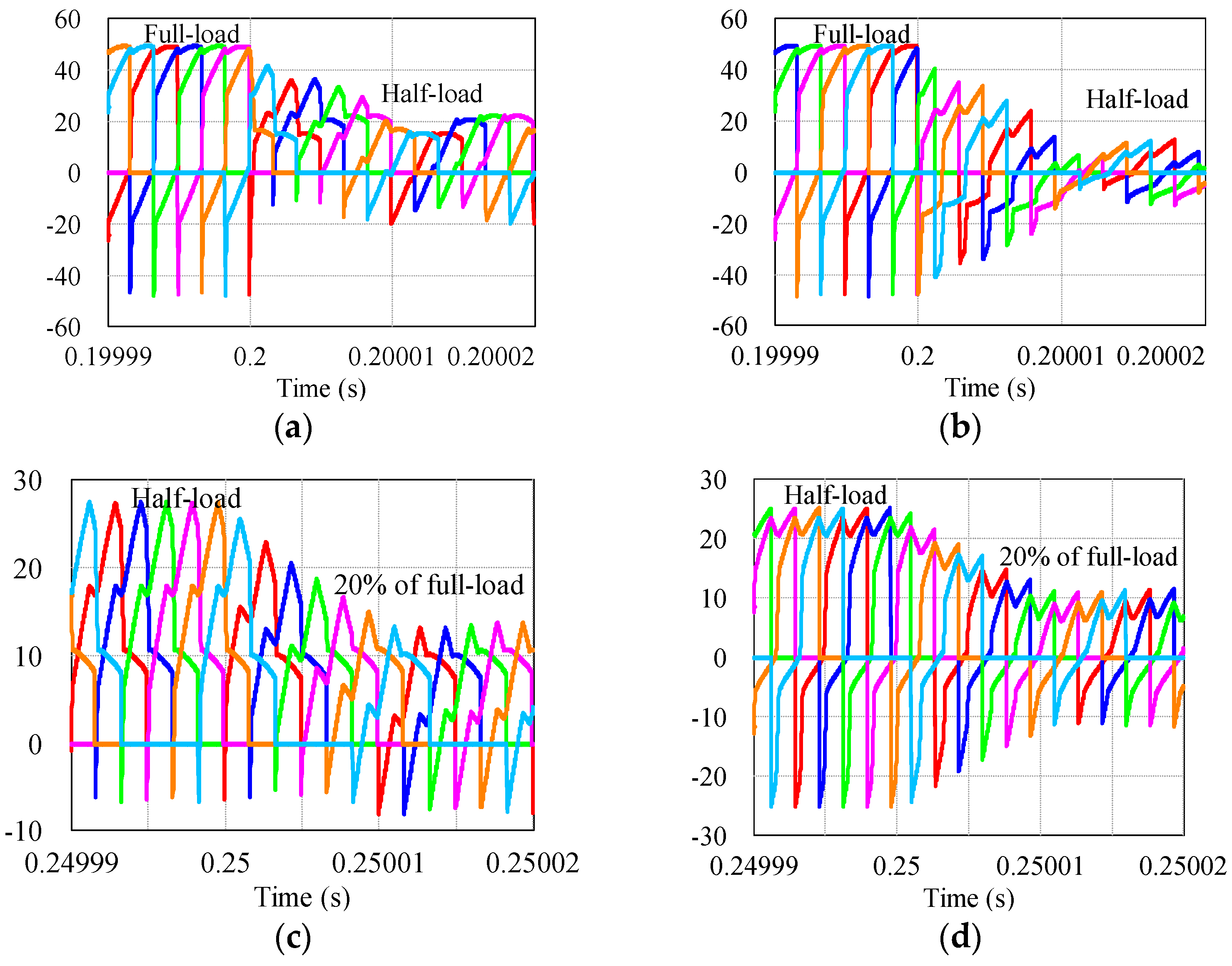
4.2. Performance Under Step Changes in Load
5. Conclusions
Author Contributions
Funding
Conflicts of Interest
Appendix A. Design Equations (A24) and (A25)

References
- Eriksson, M.; Waters, R.; Svensson, O.; Isberg, J.; Leijon, M. Wave power absorption: Experiments in open sea and simulation. JAP 2007, 102, 1–5. [Google Scholar] [CrossRef]
- Bostrom, C.; Leijon, M. Operation analysis of a wave energy converter under different load conditions. IET Trans. Renew. Power Gener. 2011, 5, 245–250. [Google Scholar] [CrossRef]
- Leijon, M.; Bernhoff, H.; Agren, O.; Isberg, J.; Sundberg, J.; Berg, M.; Karlsson, K.E.; Wolfbrandt, A. Multiphysics simulation of wave energy to electric energy conversion by permanent magnet linear generators. IEEE Trans. Energy Convers. 2005, 20, 219–224. [Google Scholar] [CrossRef]
- Kimoulakis, N.M.; Kladas, A.G.; Tegopoulos, J.A. Power generation optimization from sea waves by using a permanent magnet linear generator drive. IEEE Trans. Magn. 2008, 44, 1530–1533. [Google Scholar] [CrossRef]
- Wang, C.; Zhang, Z. Key technologies of wave energy power generation system. In Proceedings of the IEEE Conference on Mechatronics and Automation, Takamatsu, Japan, 6–9 August 2017. [Google Scholar]
- Vining, J.; Lipo, T.A.; Venkataramanan, G. Experimental evaluation of a doubly-fed linear generator for ocean wave energy applications. In Proceedings of the IEEE Energy Conversion Congress and Exposition, Phoenix, AZ, USA, 17–22 September 2011; pp. 4115–4122. [Google Scholar]
- Faiz, J.; Nematsaberi, A. Linear permanent magnet generator concepts for direct-drive wave energy converters: A comprehensive review. In Proceedings of the IEEE Conference on Industrial Electronics and Applications, Siem Reap, Cambodia, 18–20 June 2017; pp. 618–623. [Google Scholar]
- Prado, M.; Polinder, H. Direct drive in wave energy conversion-AWS full scale prototype case study. In Proceedings of the IEEE Power and Energy Society General Meeting, Detroit, MI, USA, 24–28 July 2011. [Google Scholar]
- Gemme, D.A.; Bastien, S.P.; Sepe, R.B.; Montgomery, J.; Grilli, S.T.; Grilli, A. Experimental testing and model validation for ocean wave energy harvesting buoys. In Proceedings of the IEEE Energy Conversion Congress and Exposition, Denver, CO, USA, 15–19 September 2013. [Google Scholar]
- Kimoulakis, N.M.; Kakosimos, P.E.; Kladas, A.G. Power Generation by using point absorber wave energy converter coupled with linear permanent magnet generator. In Proceedings of the Mediterranean Conference and Exhibition on Power Generation, Transmission, Distribution and Energy Conversion, Agia Napa, Cyprus, 7–10 November 2010. [Google Scholar]
- Trapanese, M.; Cipriani, G.; Corpora, M.; Di Dio, V. A general comparison between various types of linear generators for wave energy conversion. In Proceedings of the IEEE OCEANS conference, Anchorage, AK, USA, 18–21 September 2017. [Google Scholar]
- Curcic, M.; Quaicoe, J.E.; Bachmayer, R. A novel double-sided linear generator for wave energy conversion. In Proceedings of the IEEE OCEANS conference, Genova, Italy, 18–21 May 2015. [Google Scholar]
- Vermaak, R.; Kamper, M.J. Experimental Evaluation and Predictive Control of an Air-Cored Linear Generator for Direct-Drive Wave Energy Converters. IEEE Trans. Ind. Appl. 2012, 48, 1817–1826. [Google Scholar] [CrossRef]
- Hodgins, N.; Keysan, O.; McDonald, A.S.; Mueller, M.A. Design and Testing of a Linear Generator for Wave-Energy Applications. IEEE Trans. Ind. Electron. 2012, 59, 2094–2103. [Google Scholar] [CrossRef]
- Hodgins, N.; Keysan, O.; McDonald, A.; Mueller, M. Linear generator for direct drive wave energy applications. In Proceedings of the IEEE Conference on Electrical Machines, Rome, Italy, 6–8 September 2010. [Google Scholar]
- Li, Q.; Khan, F.H.; Imtiaz, A.M. Maximum power point tracking of stirling generator and ocean wave energy conversion systems using a two-stage power converter. In Proceedings of the IEEE Workshop on Control and Modeling for Power Electronics, Salt Lake City, UT, USA, 23–26 June 2013. [Google Scholar]
- Lu, S.Y.; Wang, L.; Lo, T.M. Integration of wind-power and wave-power generation systems using a DC micro grid. In Proceedings of the IEEE Industry Application Society Annual Meeting, Vancouver, BC, Canada, 5–9 October 2014. [Google Scholar]
- Lafoz, M.; Blanco, M.; Ramírez, D. Grid connection for wave power farms. In Proceedings of the European Conference on Power Electronics and Applications, Birmingham, UK, 30 August–1 September 2011. [Google Scholar]
- Garces, A.; Tedeschi, E.; Verez, G.; Molinas, M. Power collection array for improved wave farm output based on reduced matrix converters. In Proceedings of the IEEE Workshop on Control and Modelling for Power Electronics, Boulder, CO, USA, 28–30 June 2010. [Google Scholar]
- Rhinefrank, K.; Schacher, A.; Prudell, J.; Brekken, T.K.; Stillinger, C.; Yen, J.Z.; Ernst, S.G.; von Jouanne, A.; Amon, E.; Paasch, R.; et al. Comparison of Direct-Drive Power Takeoff Systems for Ocean Wave Energy Applications. IEEE J. Ocean. Eng. 2012, 37, 35–44. [Google Scholar] [CrossRef]
- Wu, F.; Ju, P.; Zhang, X.P.; Qin, C.; Peng, G.J.; Huang, H.; Fang, J. Modeling, Control Strategy, and Power Conditioning for Direct-Drive Wave Energy Conversion to Operate With Power Grid. Proc. IEEE 2013, 101, 925–941. [Google Scholar] [CrossRef]
- Qing, K.; Xi, X.; Zanxiang, N.; Lipei, H.; Kai, S. Design of grid-connected directly driven wave power generation system with optimal control of output power. In Proceedings of the European Conference on Power Electronics and Applications, Lille, France, 2–6 September 2013. [Google Scholar]
- Rao, W.F.; Zhang, B.; Pan, J.F.; Wu, X.Y.; Yuan, J.P.; Qiu, L. Voltage control strategy of DC microgrid with direct drive wave energy generator. In Proceedings of the Conference on Power Electronics Systems and Applications—Smart Mobility, Power Transfer and Security, Hong Kong, China, 12–14 December 2017. [Google Scholar]
- Nagendrappa, H. High-Frequency Transformer Isolated Fixed Frequency DC–DC Resonant Power Converters for Alternative Energy Applications. Ph.D. Thesis, University of Victoria, Victoria, BC, Canada, July 2015. [Google Scholar]
- Nagendrappa, H.; Bhat, A.K.S. A Fixed Frequency ZVS Integrated Boost Dual Three-Phase Bridge DC–DC LCL-Type Series Resonant Converter. IEEE Trans. Power Electron. 2018, 33, 1007–1023. [Google Scholar] [CrossRef]
- Steigerwald, R.L.; De Doncker, R.W.; Kheraluwala, M.H. A comparison of high power DC–DC soft-switched converter topologies. IEEE Trans. Ind. Appl. 1996, 32, 1139–1145. [Google Scholar] [CrossRef]
- Kheraluwala, M.N.; Gascoigne, R.W.; Divan, D.M.; Baumann, E.D. Performance characterization of a high-power dual active bridge DC-to-DC converter. IEEE Trans. Ind. Appl. 1992, 28, 1294–1301. [Google Scholar] [CrossRef]
- Almardy, M.S.; Bhat, A.K.S. Three-phase LCL-type series-resonant converter with capacitive output filter. IEEE Trans. Power Electron. 2011, 26, 1172–1183. [Google Scholar] [CrossRef]
- Steigerwald, R.L.; Roshen, W.; Saj, C.F. A high-density 1 kW resonant power converter with a transient boost function. IEEE Trans. Power Electron. 1993, 8, 431–438. [Google Scholar] [CrossRef]
- Gautam, D.S.; Bhat, A.K.S. An integrated boost-dual half-bridge LCL SRC with capacitive output filter for electrolyser application. In Proceedings of the IEEE Industry Electronics Society Annual Conference, Montreal, QC, Canada, 25–28 October 2012; pp. 3376–3381. [Google Scholar]
- Sabate, J.A.; Vlatkovic, V.; Ridley, R.B.; Lee, F.; Cho, B.H. Design considerations for high-voltage high-power full-bridge zero-voltage-switched PWM converter. In Proceedings of the Applied Power Electronics Conference, Los Angeles, CA, USA, 11–16 March 1990; pp. 275–284. [Google Scholar]
- AGAMY, M.; Dong, D.; Garces, L.J.; Zhang, Y.; Dame, M.; Atalla, A.S.; Pan, Y. A high power medium voltage resonant dual active bridge for DC distribution networks. In Proceedings of the IEEE Energy Conversion Congress and Exposition, Milwaukee, WI, USA, 18–22 September 2016. [Google Scholar]
- Nagendrappa, H.; Bhat, A.K.S. A Fixed Frequency ZVS Integrated Boost Dual Three-Phase Bridge DC–DC LCL-type Series Resonant Converter for large Power Applications. In Proceedings of the IEEE International Conference on Smart Grids, Power and Advanced Control Engineering, Bangalore, India, 17–19 August 2017; pp. 99–105. [Google Scholar]
- Yaqoob, M.; Loo, K.H.; Lai, Y.M. Fully Soft-Switched Dual-Active-Bridge Converter with Switched-Impedance-Based Power Control. IEEE Trans. Power Electron. 2018, 33, 9267–9281. [Google Scholar] [CrossRef]
- Cao, G.; Guo, Z.; Wang, Y.; Sun, K.; Kim, H.J. A DC–DC conversion system for high power HVDC-connected photovoltaic power system. In Proceedings of the Conference on Electrical Machines and Systems, Sydney, Australia, 11–14 August 2017. [Google Scholar]
- Suryadevara, R.; Modepalli, T.; Li, K.; Parsa, L. Three-phase current-fed soft-switching DC–DC converter. In Proceedings of the IEEE International Symposium on Industrial Electronics, Edinburgh, UK, 19–21 June 2017; pp. 899–904. [Google Scholar]
- Bernardi, P.; Cicchetti, R.; Pelosi, G.; Reatti, A.; Selleri, S.; Tatini, M. An equivalent circuit for EMI prediction in printed circuit boards featuring a straight-to-bent microstrip line coupling. Prog. Electromagn. Res. B 2008, 5, 107–118. [Google Scholar] [CrossRef]
- Hazra, S.; De, A.; Cheng, L.; Palmour, J.; Hull, B.A.; Allen, S.; Bhattacharya, S. High switching performance of 1700-V, 50-A SiC power MOSFET over Si IGBT/BiMOSFET for advanced power conversion applications. IEEE Trans. Power Electron. 2016, 31, 4742–4754. [Google Scholar] [CrossRef]


| Parameter | Value |
|---|---|
| Rated power at 0.7 m/s | 10 kW |
| Open circuit voltage (Line) at 0.7 m/s | 200 V |
| Generator resistance | 0.44 Ω |
| Generator inductance | 11.7 mH |
| Iron losses at 0.7 m/s | 0.57 kW |
| Length of air gap | 3 mm |
| Size of magnet block | 6.5 × 35 × 100 mm3 |
| Pole width | 50 mm |
| Stator sides (number) | 4 |
| Stator length (vertical) | 1.264 m |
| Translator length (vertical) | 1.867 m |
| Weight of translator | 1000 kg |
| Parameter | Value |
|---|---|
| Input voltage (Vin) | 135 V to 270 V |
| Output voltage (Vo) | 400 V |
| Output Power (Po) | 10 kW |
| DC bus voltage (Vbus) | 600 V |
| Switching frequency (fs) | 100 kHz |
| Case | Inverter (MOSFET) Losses | Rectifier Conduction Losses (W) | Transformer + Q Loss (W) (Assumed 1%) | Total Losses (W) | Efficiency (%) | |||
|---|---|---|---|---|---|---|---|---|
| Turn-off (W) | Conduction (W) | Diode (W) | ||||||
| Output | Boost | |||||||
| Vin = 135V, Full load. | 334.31 | 478.81 | 10.99 | 62.50 | 99.25 | 200.00 | 1185.86 | 89.39 |
| Vin = 270V, Full load. | 136.64 | 196.47 | 10.99 | 62.50 | 49.62 | 200.00 | 656.22 | 93.84 |
| Vin = 135V, Half load. | 70.11 | 124.10 | 0.84 | 31.25 | 49.62 | 100.00 | 375.92 | 93.00 |
| Vin = 270V, Half load. | 25.77 | 51.74 | 0.84 | 31.25 | 24.81 | 100.00 | 234.41 | 95.52 |
| Vin = 135V, 20% load. | 9.21 | 19.66 | 1.25 | 12.50 | 19.85 | 40.00 | 102.47 | 95.12 |
| Parameter | Case-1: Vin(min) = 135V, Full Load | Case-2: Vin(max) = 270V, Full Load | Case-3: Vin(min) = 135V, Half Load | Case-4: Vin(max) = 270V, Half Load | Case-5: Vin(min) = 135V, 20% Load | ||||||
|---|---|---|---|---|---|---|---|---|---|---|---|
| Cal. | Sim. | Cal. | Sim. | Cal. | Sim. | Cal. | Sim. | Cal. | Sim. | ||
| Vo (V) | 400.00 | 392.51 | 400.00 | 394.92 | 400.00 | 390.95 | 400.00 | 390.50 | 400.00 | 390.21 | |
| Io (A) | 25.00 | 24.53 | 25.00 | 24.68 | 12.50 | 12.21 | 12.50 | 12.20 | 5.00 | 4.88 | |
| Vbus (V) | 600.00 | 598.95 | 600.00 | 600.61 | 443.79 | 445.11 | 443.79 | 443.59 | 388.97 | 386.96 | |
| Vboost,DC (V) | 465.00 | 463.95 | 330.00 | 330.61 | 308.79 | 310.11 | 173.79 | 173.59 | 253.97 | 251.96 | |
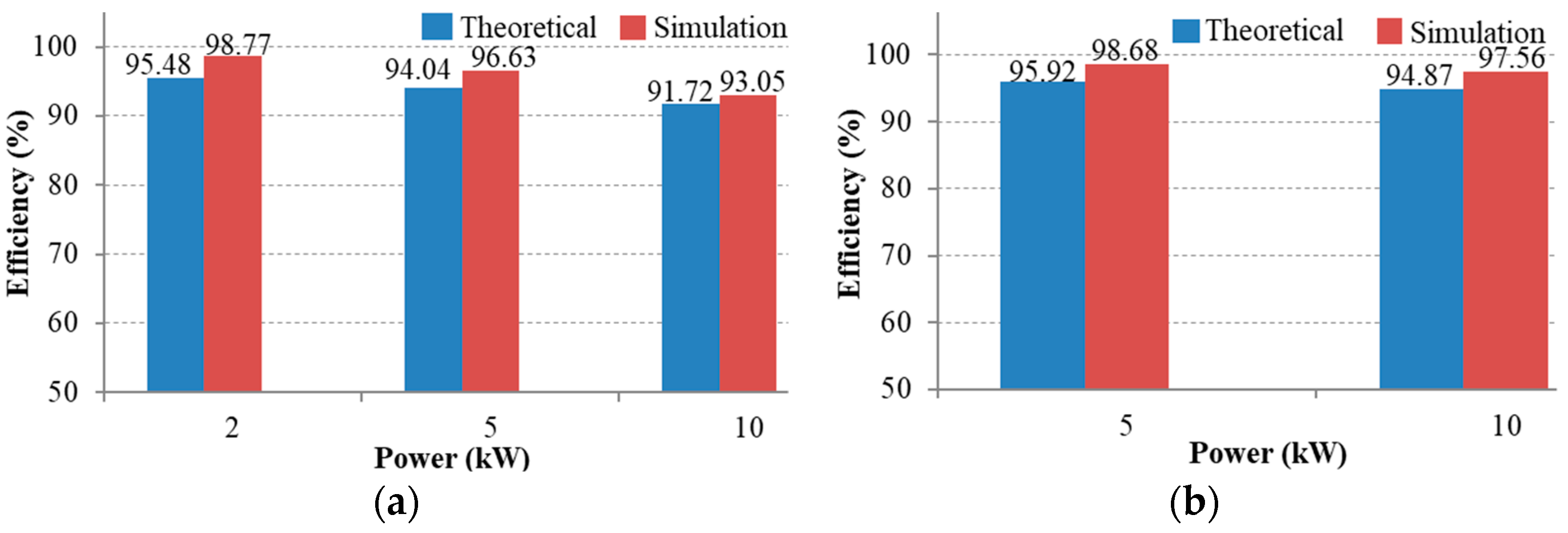
| H (%) | 91.72 | 93.05 | 94.87 | 97.56 | 94.04 | 96.63 | 95.92 | 98.68 | 95.48 | 98.77 | |
| δ (°) | 180 | 180 | 85 | 84 | 108 | 107 | 61 | 60 | 101 | 98 | |
| ILsp (ILsr) (A) | Mod 1 | 14.11 (9.97) | 13.75 (9.82) | 14.11 (9.97) | 13.81 (9.86) | 7.06 (4.99) | 6.94 (4.87) | 7.06 (4.99) | 6.93 (4.86) | 2.83 (2.00) | 2.77 (1.92) |
| Mod 2 | 14.11 (9.97) | 13.75 (9.82) | 14.11 (9.97) | 13.86 (9.88) | 7.06 (4.99) | 6.99 (4.90) | 7.06 (4.99) | 6.97 (4.89) | 2.83 (2.00) | 2.83 (1.97) | |
| VCsp (VCsr) (V) | Mod 1 | 1413.82 (999.72) | 1387.17 (985.45) | 1413.82 (999.72) | 1393.28 (986.76) | 707.41 (500.21) | 688.22 (486.58) | 707.41 (500.21) | 687.94 (487.07) | 283.57 (200.50) | 273.34 (193.28) |
| Mod 2 | 1413.82 (999.72) | 1387.34 (985.48) | 1413.82 (999.72) | 1398.43 (991.77) | 707.41 (500.21) | 693.83 (492.90) | 707.41 (500.21) | 692.48 (490.40) | 283.57 (200.50) | 280.32 (197.57) | |
| iL’p (p) (mA) | Mod 1 | 54.66 | 56.33 | 54.66 | 56.73 | 54.66 | 56.14 | 54.66 | 56.04 | 54.66 | 56.03 |
| Mod 2 | 54.66 | 56.29 | 54.66 | 56.69 | 54.66 | 56.14 | 54.66 | 56.10 | 54.66 | 56.04 | |
© 2019 by the authors. Licensee MDPI, Basel, Switzerland. This article is an open access article distributed under the terms and conditions of the Creative Commons Attribution (CC BY) license (http://creativecommons.org/licenses/by/4.0/).
Share and Cite
Harischandrappa, N.; Bhat, A.K.S. A 10 kW ZVS Integrated Boost Dual Three-Phase Bridge DC–DC Resonant Converter for a Linear Generator-Based Wave-Energy System: Design and Simulation. Electronics 2019, 8, 115. https://doi.org/10.3390/electronics8010115
Harischandrappa N, Bhat AKS. A 10 kW ZVS Integrated Boost Dual Three-Phase Bridge DC–DC Resonant Converter for a Linear Generator-Based Wave-Energy System: Design and Simulation. Electronics. 2019; 8(1):115. https://doi.org/10.3390/electronics8010115
Chicago/Turabian StyleHarischandrappa, Nagendrappa, and Ashoka K. S. Bhat. 2019. "A 10 kW ZVS Integrated Boost Dual Three-Phase Bridge DC–DC Resonant Converter for a Linear Generator-Based Wave-Energy System: Design and Simulation" Electronics 8, no. 1: 115. https://doi.org/10.3390/electronics8010115