Drift-Diffusion Simulation of High-Speed Optoelectronic Devices


Southern Federal University, Institute of Nanotechnology, Electronics and Electronic Equipment Engineering, 2 Shevchenko St., Taganrog 347922, Russia
*
Author to whom correspondence should be addressed.
Electronics 2019, 8(1), 106; https://doi.org/10.3390/electronics8010106
Submission received: 30 December 2018
/
Revised: 14 January 2019
/
Accepted: 15 January 2019
/
Published: 18 January 2019
(This article belongs to the Section Microelectronics)
Abstract
:In this paper, we address the problem of research and development of the advanced optoelectronic devices designed for on-chip optical interconnections in integrated circuits. The development of the models, techniques, and applied software for the numerical simulation of carrier transport and accumulation in high-speed AIIIBV (A and B refer to group III and V semiconductors, respectively) optoelectronic devices is the purpose of the paper. We propose the model based on the standard drift-diffusion equations, rate equation for photons in an injection laser, and complex analytical models of carrier mobility, generation, and recombination. To solve the basic equations of the model, we developed the explicit and implicit techniques of drift-diffusion numerical simulation and applied software. These aids are suitable for the stationary and time-domain simulation of injection lasers and photodetectors with various electrophysical, constructive, and technological parameters at different control actions. We applied the model for the simulation of the lasers with functionally integrated amplitude and frequency modulators and uni-travelling-carrier photodetectors. According to the results of non-stationary simulation, it is reasonable to optimize the parameters of the lasers-modulators and develop new construction methods aimed at the improvement of photodetectors’ response time.
1. Introduction
Nowadays, on-chip metal interconnections are very close to the physical limit of their application in state-of-the-art integrated circuits (ICs). It is caused by the appreciable degradation of response time, energy and technological efficiency, channel capacity, noise immunity, reliability, and other characteristics of integrated metal conductors at dimensions within several tens of nanometers and less, which are typical for modern integrated electronics [1]. The sustainable progress in IC production technology requires the immediate solution of the interconnection problem. It can be performed by means of the development of new interconnection types or optimization and modification of traditional interconnecting techniques. Both approaches have advantages and disadvantages and evolve concurrently.
This paper is focused on the research and development of novel high-performance on-chip interconnections for next-generation ICs. Super- and nanoconductors, radio frequency and optical commutation lines, carbon nanotubes, and graphene are the promising types of advanced integrated interconnections [2,3,4,5]. However, optical interconnecting is characterized by some important advantages over its counterparts and can solve the problem for various integrated devices in the immediate future [6,7,8].
The optoelectronic approach deals with the constructive and technological integration of optical interconnections with silicon-based electronic IC elements. Typical on-chip optical interconnection consists of a source of optical radiation, a high-speed modulator, an integrated waveguide, and a photodetector. Optoelectronics has made significant progress in the improvement of these devices, but a set of theoretical and practical problems remains unsolved. As of now, on-chip optoelectronic systems are suitable for highly specialized devices with sufficiently large scales or high-levels of interconnection in ICs. For example, optical interconnections can be used for the inter-core commutation in multi-core ultra-large-scale ICs [9].
Silicon photonics seem to be one of the advanced research directions in the field of IC optical interconnection [10,11,12]. This approach provides some important benefits, such as small losses, adaptability to streamlined manufacture, and high efficiency of waveguides. The main problem of silicon photonics is the development of on-chip optical radiation sources. This problem remains unsolved and causes the relevance of the design of hybrid AIIIBV-silicon systems [13,14,15] (A and B refer to group III and V semiconductors, respectively).
In this paper we consider the modelling of dynamic characteristics of AIIIBV high-speed optoelectronic devices for on-chip optical interconnections in ICs. The development of the appropriate model, simulation technique, and software is the purpose of the research.
The semiclassical and quantum-mechanical methods are the essential approaches to the simulation of semiconductor devices in modern computational electronics [16]. We propose to apply the drift-diffusion approximation of the semiclassical approach for the simulation of lasers and photodetectors. In spite of several limitations, it is utilized for the research of semiconductor devices and allows us to obtain adequate simulation results [17].
2. Models
In this paper we propose a numerical model designed for the simulation of charge carrier transport in high-speed AIIIBV optoelectronic devices within the drift-diffusion approximation of the semiclassical approach [16]. The model includes the following basic differential equations:
- The drift-diffusion equations for the electron and hole current densities and [18]:where is the electron charge; , are the electron and hole mobilities; , are the electron and hole densities; is the electrostatic potential; , are the heterostructure potentials in the conduction and valence bands of a semiconductor; is the temperature potential;
- The continuity equations for electrons and holes [18]:where is time; , are the generation and recombination rates of electron-hole pairs;
- The Poisson’s equation for electrostatic field [18]:where is the dielectric permittivity of a semiconductor; is the permittivity of vacuum; , are the densities of ionized donors and acceptors;
- The rate equation for photons in an injection laser [19]:where is the photon density; is the photon lifetime in the resonant cavity of a laser; is the fraction of spontaneous emission in the laser mode; is the intrinsic carrier concentration; is the time constant of spontaneous recombination; is the photon velocity in the active region of a laser; is the optical gain coefficient.
If one considers a photodetector, it is enough to solve Equations (1)–(5), which represent the standard drift-diffusion formulation. The simulation of an injection laser requires the solution of additional Equation (6), describing the dynamics of photons leaving from the resonant cavity and photon generation caused by the spontaneous and stimulated radiative recombination of charge carriers.
To calculate heterostructure potentials and , the following formulas are used:
where , are the potentials of conduction band bottom and valence band top; , are the reference potentials of the corresponding bands. It is reasonable to choose the minimum of and maximum of in the energy band diagram of a heterostructure as the reference potentials for Equation (7). The data required for the band structure calculations are represented in [20].
The optical gain coefficient in Equation (6) depends on charge carrier and photon concentrations and in the active region of the laser. Traditionally, it is defined by the following analytical model [19]:
where is the proportionality factor; is the resulting factor of optical gain reduction; is the factor of optical confinement; , , are the coefficients of the trap, radiative, and Auger recombination; is the threshold carrier concentration; , are the quasi-Fermi levels for electrons and holes. In Equation (8), as well as in Equation (6), the generalized carrier concentration is replaced by the expression , which takes into account the electron, hole, and photon densities.
The following Dirichlet boundary conditions for Equations (1)–(6) are applied at ohmic and Schottky contacts in the case of fixed voltage mode [21]:
where is the Schottky barrier height (at ohmic contacts ); is the bias voltage applied to a contact at the moment . Equations (9)–(11) were derived under the assumptions of thermodynamic equilibrium and infinite recombination velocity at a contact.
If the fixed current mode is considered, the boundary conditions in Equations (9), (10), and (12) remain unchanged, and Equation (11) is replaced by the following formula [22]:
where is the normal to the surface of a contact; is the density of current flowing through a contact at the moment .
At the contact-free boundaries of a device, the following Neumann conditions are set [22]:
To obtain the proper initial conditions for the non-stationary drift-diffusion model, the stationary formulation of Equations (1)–(6) should be solved numerically.
In this research, we apply the following analytical models for the calculation of charge carrier mobilities and :
- The Caughey–Thomas model, which takes into account the dependence of electron and hole mobilities on the lattice temperature and impurity concentrations and [20]:where is the type of conductivity ( or ); , , , , are the material-dependent fitting parameters;
- The model of high-field hole mobility, which describes the effect of hole drift velocity saturation [20]:where is the Caughey–Thomas mobility of holes; is the gradient of quasi-Fermi level for holes; is the saturation velocity of holes; is the material-dependent fitting parameter;
- The model of high-field electron mobility, which addresses the overshoot and saturation of field-velocity characteristics for electrons in AIIIBV semiconductors [20]:where is the Caughey–Thomas mobility of electrons; is the gradient of quasi-Fermi level for electrons; is the saturation velocity of electrons in the upper valley; is the material-dependent fitting parameter; is the critical field intensity, at which the electron drift velocity reaches the maximum.
It is worth noting that the mobility models in Equations (15)–(19) are phenomenological. It means that the models are suitable for the adequate estimation of high-field effects, but their accurate simulation requires the experimentally measured mobility or application of the hydrodynamic approach.
We take into account the following processes of carrier recombination in high-speed AIIIBV optoelectronic devices:
- The stimulated radiative recombination in a laser [19]:
- The spontaneous radiative recombination in a laser [19]:
- The Auger recombination [20]:where , are the material-dependent Auger coefficients for electrons and holes;
- The direct recombination in materials with a direct bandgap [20]:where is the material-dependent coefficient of the direct recombination.
We neglect the Shockley–Read–Hall recombination because its inertness is more durable than the time intervals being considered [20]. Furthermore, in direct bandgap materials, that process dominates only under conditions of very low carrier density [23].
The following analytical model is usually utilized for the calculation of the optical generation rate in resonant-cavity-enhanced (RCE) photodetectors [21]:
where is the power of incident optical radiation at the moment ; is the quantum efficiency of a device; is the volume of the absorption region of a photodetector; is the photon energy equal to the bandgap energy of the absorption region; , are the reflection coefficients of the semi- and totally-reflecting mirrors, which form a resonant cavity; is the absorption coefficient of a semiconductor; is the length of a resonator. Equation (25) is valid at resonant wavelengths , where is a positive integer and gives the peak value of quantum efficiency. The model in Equations (24) and (25) assumes the instant propagation of light throughout a resonant cavity and does not take into account the coordinate variation of the optical generation rate. In two- and three-dimensional cases, the last feature leads to the overestimated results of photoresponse calculation.
In this paper we propose an improved model for the calculation of the optical generation rate in RCE photodetectors.
If a monochromatic light propagates through a semiconductor material, the absorption is described by the Beer–Lambert–Bouguer law [24]:
where is the thickness of the absorbing layer; is the intensity of the incoming light beam; is the intensity of an outgoing light beam; is the absorption coefficient of a semiconductor at the wavelength of incident light.
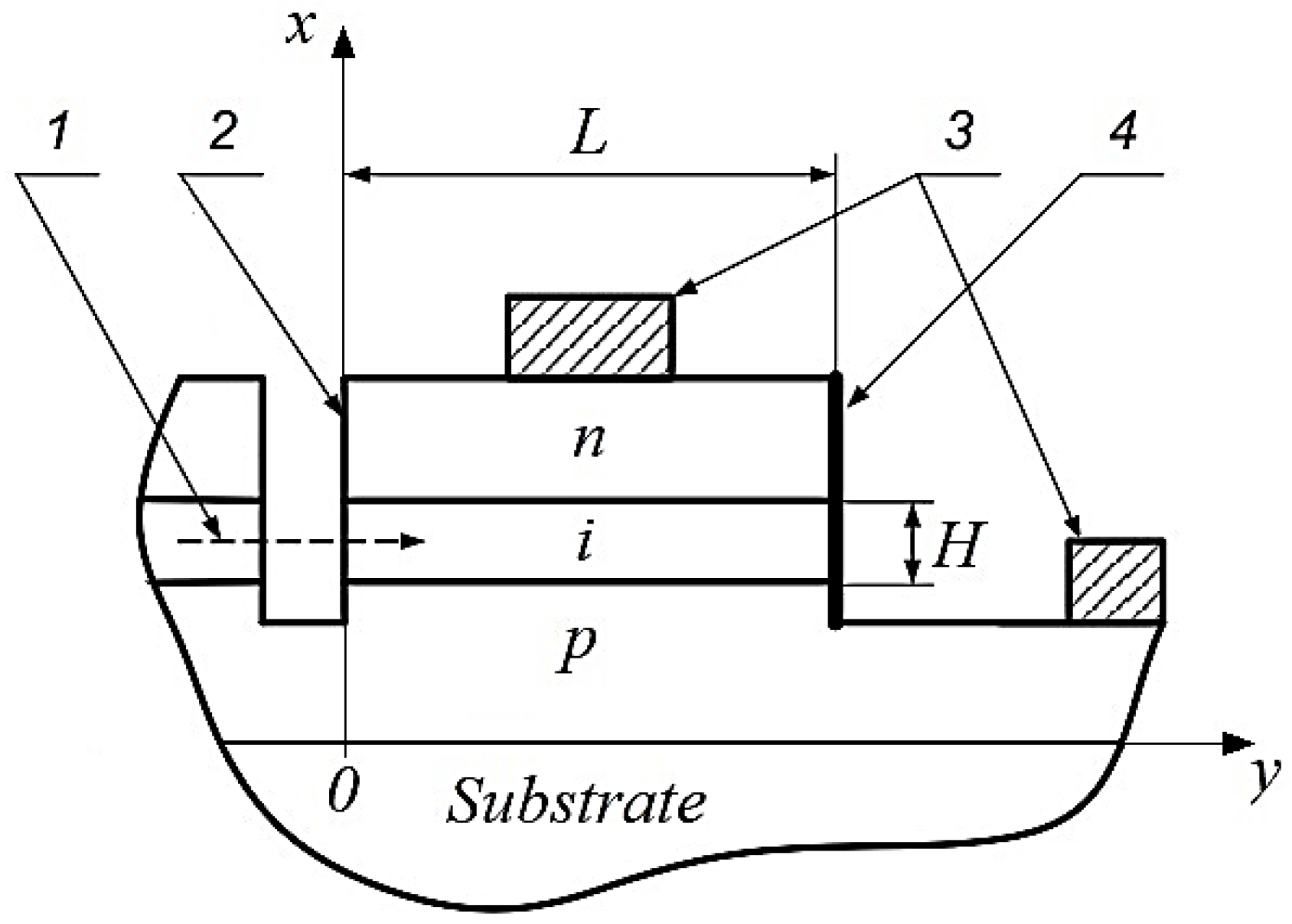
Here we consider the waveguide p-i-n RCE photodetector shown in Figure 1. The resonant cavity is formed by semi- and totally-reflecting mirrors (positions 2 and 4). The laser beam (position 1) with time-dependent power falls orthogonally to the surface of semi-reflecting mirror (position 2). The coordinate axis is directed along the incident laser beam and has the reference point near the semi-reflecting mirror. Outside of the resonant cavity, the photon density is given by the following equation:
where is the speed of light in vacuum; is the photon energy equal to the bandgap energy of the absorption region; , are the width and height of the resonant cavity or absorption region, as shown in Figure 1. After the passing of light through the semi-reflecting mirror, the photon density at the distance and the moment is defined by the following formula resulting from Equation (26):
where is the refractive index of the absorption region; is the instant, at which photons overcome the distance in the resonant cavity. The reduction of photon density caused by the absorption and -fold reflection of light from the resonator mirrors is described by the following equation:
where is the multiplicity of photon beam reflection; , are the floor and ceiling functions. In the case of one-dimensional simulation along the axis, the total optical power absorbed in the whole resonant cavity and optical generation rate are given by the following formulas:
where is the time step. Otherwise, in Equation (30) should be replaced by , where is the step of coordinate grid along the axis, and in Equation (31) should be replaced by , where is the step of coordinate grid along the axis.
The model in Equations (29)–(31) is suitable for one- and two-dimensional non-stationary simulation of high-speed RCE photodetectors and takes into account the dynamics of photon propagation in the resonant cavity. The model does not consider wave effects, but the introduction of special fitting parameters in Equation (30) allows us to fit the model to the experimental data.
3. Simulation Techniques
The implementation of the model in Equations (1)–(6), with the boundary conditions in Equations (9)–(14) and the additional parameter models in Equations (7), (8), (15)–(31), requires the application of numerical methods.
To provide a stable and convergent numerical solution of a system of differential equations, an efficient discretization scheme and a high-performance algorithm are needed. These application-oriented components form a technique of numerical simulation. The development of a simulation technique implies the application of various mathematical methods and approaches, the design of applied software, and the conduction of computational experiments.
Nowadays, a lot of problems in the field of computational electronics remains unsolved. In our opinion, the universal approach to the efficient implementation of the drift-diffusion models has not been developed yet. The non-stationary simulation of heterostructural devices is characterized by the following challenges:
- The instability of discretization schemes and algorithms;
- Significant time and resource consumption;
- The inadequacy of simulation results caused by calculation errors.
Sometimes, it is quite difficult to deal with these challenges due to the features of the drift-diffusion model, the variety of parameter values, and the lack of appropriate mathematical investigations.
In this paper, we propose two techniques designed for the numerical simulation of high-speed optoelectronic devices within the drift-diffusion approximation. Both techniques are based on the finite difference method [25], in which derivatives are approximated by the finite difference expressions. The first technique applies the explicit, upwind, and Gummel’s methods and is suitable for one- and two-dimensional non-stationary simulation of lasers and photodetectors. The second one is based on the implicit, Newton’s, and Slotboom’s methods and is suitable for two-dimensional stationary simulation of lasers and photodetectors and one-dimensional non-stationary simulation of photosensitive devices. The distinctive features of the proposed simulation techniques are discussed below.
3.1. Explicit Technique
The explicit simulation technique applies the combined variable base of , where and . It is necessary for the reduction of computational error caused by the difference between the magnitude orders of carrier densities and electrostatic potential. The transformation equations for electron and hole concentrations have the following form [26]:
Current density Equations (1) and (2) are considered in terms of the Slotboom’s variable base of [27], and Equations (3)–(5) are considered in terms of the standard variable base of . After the substitution of Equations (1) and (2) in Equations (3) and (4) and the scaling of all equations by the standard factors [17,18], the drift-diffusion formulation in terms of is given by
To discretize Equations (34) and (35), we use the explicit difference scheme [28] for the time derivatives, and the first-order upwind scheme [29] for the coordinate derivatives. Equation (36) is discretized as usual. In the two-dimensional case, the resulting finite difference equations have the following form:
where , are the indexes of coordinate grid points on the y and x axes; is the index of time grid points; is the i-th step of coordinate grid along the x axis; is the j-th step of coordinate grid along the y axis; is the k-th step of time grid.
To solve the system formed by finite-difference Equations (37)–(39), we use the modified Gummel’s iterative method [30]. At each time step we calculate carrier concentrations according to Equations (37) and (38), and then we solve the system of linear algebraic equations (SLAE) in order to compute the distribution of electrostatic potential. Carrier mobilities, and generation and recombination rates for the next instant are estimated after the solution of the Poisson’s equation at the actual moment of time. In paper [21] we showed that the application of Gummel’s method together with the explicit and upwind difference schemes allows for the reduction in consumption of computational resources, but requires a shorter time step than other approaches.
If the explicit technique is utilized for the simulation of an injection laser, Equation (6) is added to the basic drift-diffusion formulation. After the scaling and explicit discretization, the rate equation for photons has the following form:
The calculation of photon density is performed after the solution of the Poisson’s equation at each time step.
3.2. Implicit Technique
The implicit technique of the drift-diffusion numerical simulation applies the Slotboom‘s variable base of , which allows us to reduce the computational error and calculate the adequate coordinate distributions of current density. The technique requires the setting of boundary conditions for and , which are given by the following equations:
- At ohmic and Schottky contacts:
- At contact-free boundaries:
The discretization scheme is based on the implicit method [28] and central differences. In the two-dimensional case, the normalized finite difference drift-diffusion equations have the following form:
To solve the system formed by finite difference Equations (44)–(46), we apply the standard Newton’s method [25]. At each instant of time, the continuity equations together with the Poisson’s one are solved iteratively. After the solution, carrier mobilities, and generation and recombination rates are recalculated for the next iteration step. The aforementioned approach is characterized by quadratic convergence (about several tens of iterations are necessary) but requires a lot of computational resources for the processing of large matrixes. That is why we do not recommend it for non-stationary two-dimensional simulation.
4. Simulation Results and Discussion
We developed the specialized software package for the numerical simulation of carrier transport and accumulation in high-speed on-chip optoelectronic devices based on AIIIBV heterostructures. The package implements the drift-diffusion model and finite difference simulation techniques discussed above. We wrote the program in the Octave programming language and executed it using the GNU Octave software. The proposed modelling aids allow the simulation of photodetectors and injection lasers with various electrophysical, constructive, and technological parameters operating at different control actions.
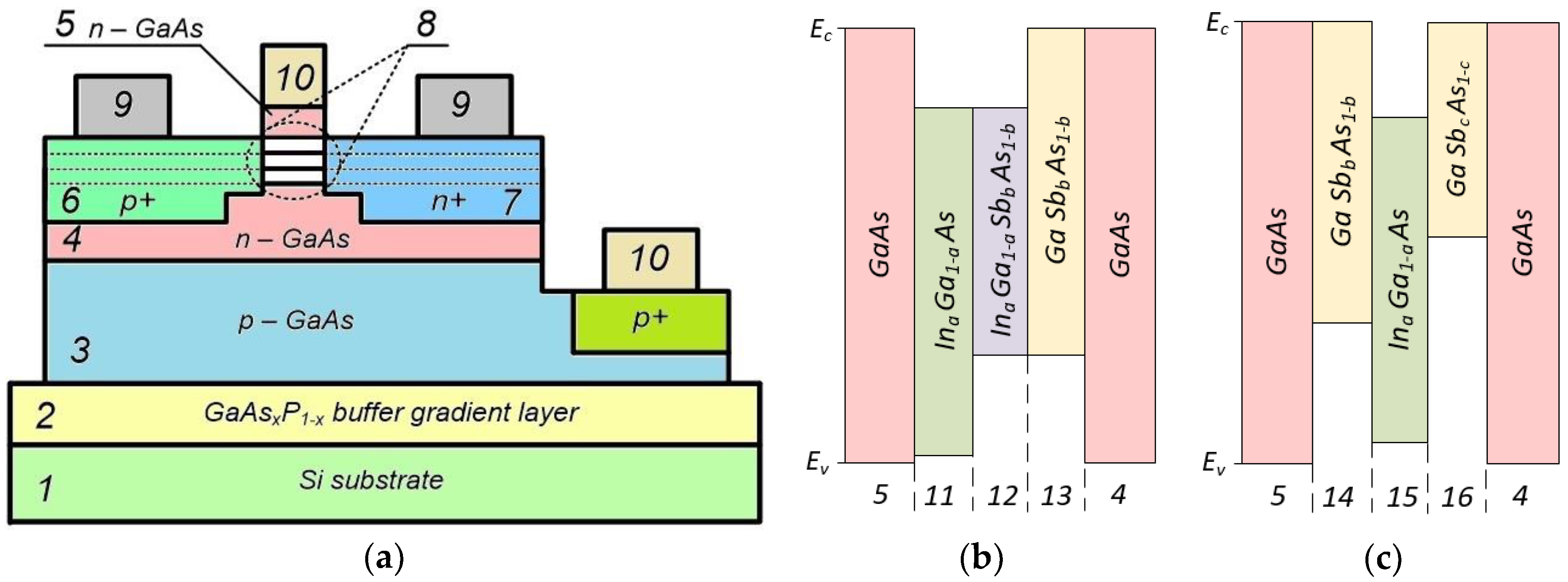
Figure 2a shows the cross-section of the injection laser with a functionally integrated modulator based on a double AIIIBV nanoheterostructure.
The laser-modulator applies the principle of the controlled spatial relocation of charge carrier density peaks within quantum regions of valence and conduction bands for the generation of amplitude- or frequency-modulated optical signals [31]. Unlike conventional laser diodes, the laser-modulator consists of heavily-doped p+ and n+ regions, as shown in positions 4 and 5 in Figure 2, with the power contacts (position 8), the amplitude or frequency modulator (position 6) with the control contacts (position 9), and the Schottky (positions 5 and 10) and p-n (positions 3 and 4) junctions. The aforementioned design provides the alteration of intensity or wavelength of laser radiation by means of the change in the transverse field applied to the control contacts (position 9). During the operation of the device, the pumping current remains unchanged.
In this paper, we considered two types of the laser-modulator. The first one includes the amplitude modulator with the energy band diagram represented in Figure 2b. The second one has the frequency modulator shown in Figure 2c. The operation principles and structures of the aforementioned types of the laser-modulator are thoroughly addressed in papers [31,32,33,34]. Since the pumping current does not change during the operation, the peak modulation frequency of the devices is not limited by slow transients in the power circuit. The performance is determined by the inertness of controlled relocation of carrier density maximums between the quantum wells of heterostructures.
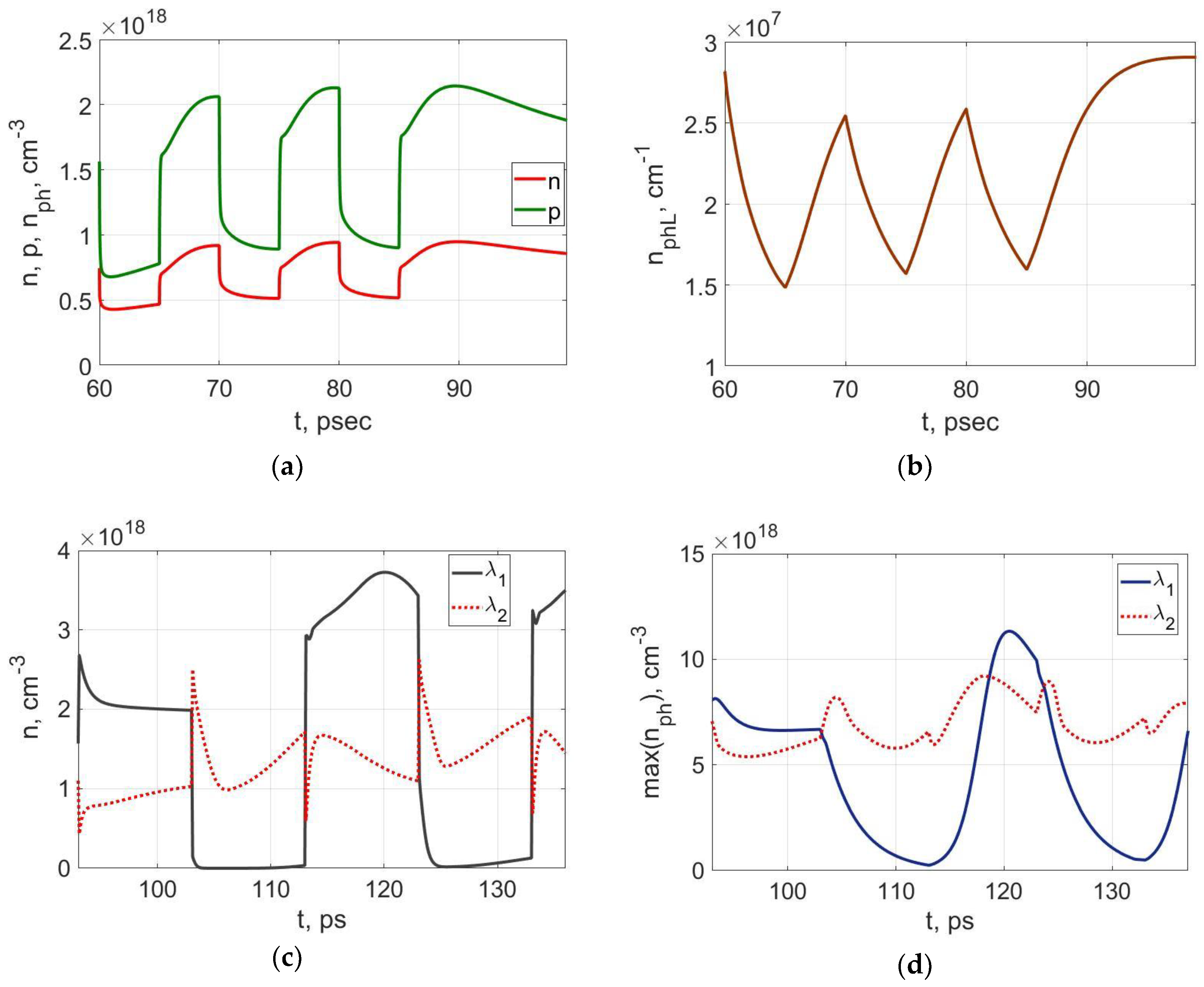
Figure 3a,b show the results of drift-diffusion two-dimensional numerical simulation of transients in the laser with a functionally integrated amplitude modulator. The active region of the device is formed by the spatially displaced quantum wells in conduction, as shown in positions 11 and 12 in Figure 2b, and valence (positions 12 and 13) bands. The configuration of the wells is such that they intersect each other at the thin narrow-bandgap region (position 12). In the operation mode being considered, the change of control voltage at constant pumping current leads to the spatial relocation of electron and hole density peaks within the quantum wells. During that process, the total number of charge carriers in the wells remains nearly unchanged. If the maximums of electron and hole densities are shifted to the overlap region (position 12) by the control electric field, the raising of the laser radiation intensity occurs. On the contrary, the relocation of carrier density peaks to the space division regions (positions 11 and 13), resulting in the reduction of intensity of generated optical radiation. The curves in Figure 3a demonstrate the dynamics of electron and hole concentrations in the region of quantum well overlap (position 12).
In Figure 3a,b, the series of 5-ps pulses is applied to the control contacts at the instant of 60 ps. Before that, the supply transient occurred due to the application of the fixed pumping current to the power contacts. The variation of control voltage leads to the relocation of electron and hole density maximums within the potential wells of the heterostructure, as shown in Figure 3a. This process results in the change of photon linear density represented in Figure 3b. According to the results, the duration of electron and hole relocations are very short and do not exceed 0.1 ps. However, the response of photon density is 50 times slower than the carrier one. This feature is caused by the durable lifetime of photons in the resonant cavity of the laser-modulator (). The shortening of is very problematic because it leads to the growth of the threshold pumping current density and degradation of some other parameters.
Figure 3c,d show the results of time-domain drift-diffusion two-dimensional simulation of the laser with a functionally integrated frequency modulator. The active region of the device consists of two quantum wells in the valence band, as shown in positions 14 and 16 in Figure 2c, and one quantum well in the conduction band (position 15). The quantum wells in the valence band have different depths depending on b and c coefficients of GaSbbAs1-b and GaSbcAs1-c solid solutions. Regions 14, 15, and 16, as shown in Figure 2c, form two heterojunctions with staggered gaps (type II) and different bandgap energies at boundaries 14-15 (boundary between regions 14 and 15) and 15-16. The wavelength of generated laser radiation is specified by the direction of the control electric field. At one direction, the peaks of electron and hole densities are relocated to the 14-15 boundary, and the laser-modulator generates the radiation with wavelength. At the opposite direction, the maximums are overlapped at the 15-16 boundary, and the device generates the radiation with wavelength. Analogously to the laser with amplitude modulation, the total number of charge carriers in the quantum wells remains nearly unchanged during the device operation.
In Figure 3c,d, the interval between the reference time and the instant of 93 ps corresponds to the transient process in the power-supply circuit of the laser-modulator. The pumping current density of 3∙105 A/cm2 and zero control voltage remain unchanged during the supply transient. Operation mode of the device starts at 93 ps and lasts until 137 ps. During this period, we apply the rectangular voltage pulses with the amplitude of 1 V to the control contacts. The duration of each pulse is 10 ps. The pumping current density is not changed. The time of the carrier density peak relocation in the quantum wells of the laser-modulator takes less than 0.1 ps, as shown in Figure 3c. This process is controlled by the transverse electric field. Therefore, the relocation is a rapid process which does not limit the modulation frequency of laser radiation. The simulation results demonstrate that the aforementioned characteristic is affected by the photon lifetime in the resonant cavity of the laser-modulator. In the case being considered, the photon lifetime is the same as for the device with the amplitude modulation. Consequently, the duration of the modulating pulse of control voltage should be more than 3 ps in order to provide the adequate modulation coefficient.
Figure 4 shows the results of the application of the model in Equations (29)–(31) for the simulation of transients in the GaAs p-i-n RCE photodiode, as shown in Figure 1. The device is illuminated by 0.2-ps rectangular optical pulses at the moments of 0 and 0.4 ps. The maximum power of the laser radiation outside the resonator is about 1 mW. The reflection coefficients of the semi- and totally-reflecting mirrors are 0.5 and 0.99. The length, height, and width of the resonant cavity are 4000, 200, and 1000 nm.
Figure 4a–c demonstrate the dynamics of photon propagation through the resonant cavity of the photodiode, which is taken into account by the model in Equations (29)–(31). In Figure 4a,b, the first pass of photons through the resonant cavity is shown. Figure 4c represents the near-stationary state after the end of resonator transient. In this state, the further change of photon concentration is insignificant. In Figure 4d, the time dependence of the optical power absorbing by the whole resonant cavity is shown. According to the curve, the duration of the transient caused by the finite velocity of photons in the resonator is about 0.1 ps. If the input optical power grows gradually due to the inertness of the laser-modulator, the resonant cavity transient is more durable and significantly affects the performance of the photodetector.
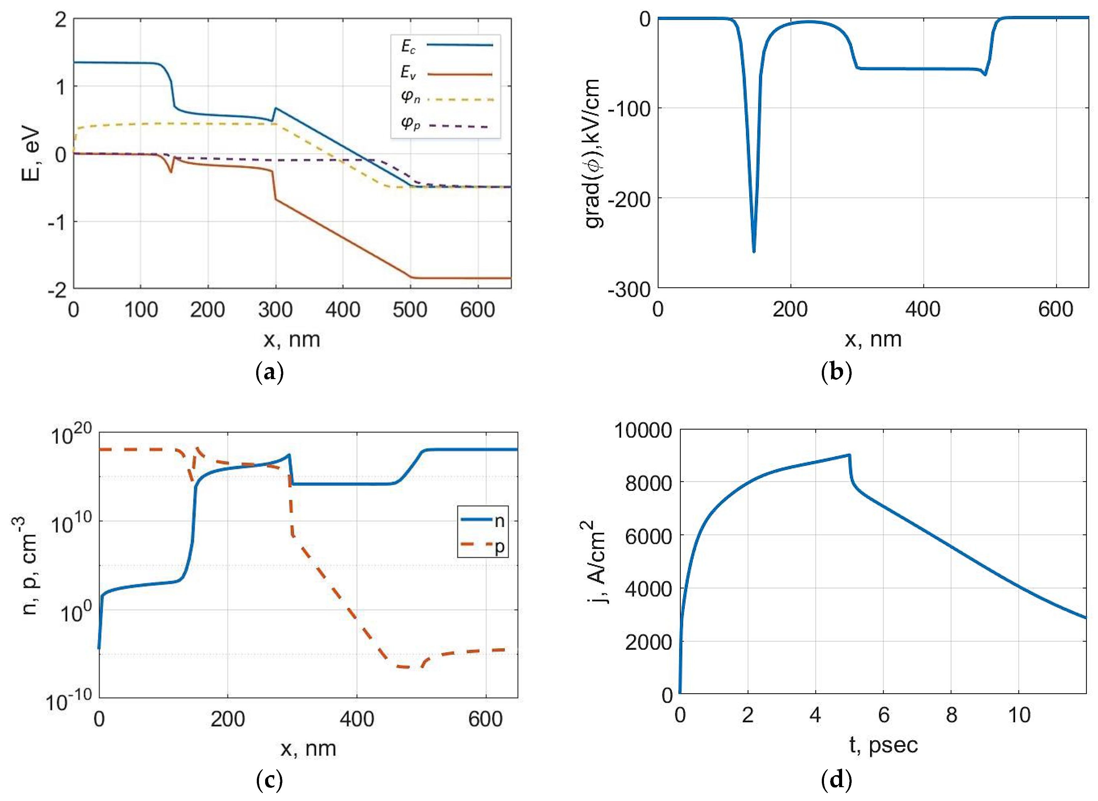
Figure 5 represents the results of non-stationary drift-diffusion simulation of the uni-travelling-carrier (UTC) photodiode [35] based on InP/In0.53Ga0.47As heterojunctions. UTC photodiodes utilize only electrons as active carriers and, in general, provide better performance (about 1 ps and less according to [36]) than conventional p-i-n photodetectors. That is why UTC diodes are promising devices for the operation as parts of on-chip optical interconnections together with the high-speed lasers-modulators. In Figure 5, the lengths of the p-type absorption and i-type collection layers are 150 and 200 nm. The device is illuminated by 5-ps rectangular laser pulse at the initial time moment. The maximum power of the laser radiation outside the resonant cavity is about 0.3 mW. The photodetector operates in the fixed voltage mode, and the absolute value of the reverse bias voltage equals 0.5 V. The length of the resonant cavity is 1000 nm. The light propagates orthogonally to the direction of the built-in electric field (analogously to the p-i-n photodetector shown in Figure 1).
Figure 5a–c show the energy band diagram of the UTC photodiode being considered and spatial distributions of electric field intensity and of carrier concentrations in its structure. The results are computed at the moment of 4.8 ps after the start of illumination. The graphs demonstrate the effect of electric field screening, which occurs in the absorption region of the photodetector at quite high powers of absorbing laser radiation. If the device is illuminated during several picoseconds and the carrier leaving is sufficiently slow, the significant quantities of photogenerated electrons and holes are accumulated in the absorption region, as shown in Figure 5c. The presence of excess charge carriers causes the damping of the built-in electric field in the device according to Figure 5b. The screening effect leads to the growth of carrier mobility and to the reduction of drift carrier transport within the absorption region.
Figure 5d demonstrate the photoresponse of the aforementioned UTC photodetector to the illumination by the rectangular laser pulse. The front edge of the photocurrent pulse can be divided into two intervals. The first one is characterized by a steep slope and lasts from 0 till approximately 1 ps. The second interval has a shallow slope and lasts from 1 ps till the end of illumination at 5 ps. During the second interval, carrier transport in the UTC photodiode is affected by the electric field screening. The back edge of the photocurrent pulse is slower than the front one due to the aforementioned screening effect. Several picoseconds are necessary for the clean-out of excess photogenerated carriers and for the recovery of the built-in electric field.
5. Conclusions
In this paper we proposed the complex model designed for one- and two-dimensional simulation of the transients and stationary states in AIIIBV high-speed optoelectronic devices. The model is based on the drift-diffusion approximation of the semiclassical approach to the description of carrier transport and accumulation in semiconductor devices. It includes the basic drift-diffusion formulation, rate equations for photons in an injection laser, Dirichlet and Neumann boundary conditions for the fixed voltage and current modes, and additional analytical models for carrier mobilities, and generation and recombination rates.
To implement the model, we developed two techniques of computer-aided numerical simulation. The first one exploits the explicit, first-order upwind, and Gummel’s methods. It is characterized by resource efficiency, but requires a very short time step for the stable solution of the equations. We applied the explicit technique for two-dimensional non-stationary simulation of the lasers-modulators and photodetectors. The second technique is based on the implicit difference scheme and Newton’s method. It provides the quadratic convergence of a numerical solution, but takes a lot of computational resources due to the simultaneous solution of three differential equations. We used the implicit technique for the computation of initial conditions and one-dimensional time-domain simulation of the high-speed photodetectors.
We developed a specialized software package for the implementation of the proposed models and numerical simulation techniques. It allows for the simulation of injection lasers and photodetectors with various electrophysical, constructive, and technological parameters operating at different control actions.
The proposed simulation aids can be used for the development of new optoelectronic devices, estimation of their expected characteristics, and optimization of basic parameters.
We performed the numerical drift-diffusion simulation of the lasers with functionally integrated optically modulators and UTC photodetectors. According to the obtained results, it is reasonable to continue the research of the lasers-modulators and optimize their parameters, especially the lifetime of photons in the resonant cavity. Besides that, the application of the lasers-modulators as parts of on-chip optical interconnections in ICs requires the development of the advanced methods aimed at the reduction of response time of high-speed photosensitive devices.
Author Contributions
I.P. and E.R. developed the model and software and wrote the paper. E.R. designed the explicit technique of numerical simulation and performed the simulation of the lasers-modulators. I.P. developed the implicit technique of numerical simulation and performed the simulation of the photodetectors.
Funding
This research was funded by the Russian Foundation for Basic Research, grant number 18-37-00432.
Conflicts of Interest
The authors declare no conflict of interest. The funders had no role in the design of the study; in the collection, analyses, or interpretation of data; in the writing of the manuscript, or in the decision to publish the results.
References
- Ceyhan, A.; Naeemi, A. Cu interconnect limitations and opportunities for SWNT interconnects at the end of the roadmap. IEEE Trans. Electron Dev. 2013, 60, 374–382. [Google Scholar] [CrossRef]
- Nossek, J.A.; Russer, P.; Noll, T.; Mezghani, A.; Ivrlac, M.T.; Korb, M.; Mukhtar, F.; Yordanov, H.; Russer, J.A. Chip-to-Chip and On-Chip Communications. In Ultra-Wideband Radio Technologies for Communications, Localization and Sensor Applications; Thomä, R., Knöchel, R.H., Sachs, J., Willms, I., Zwick, T., Eds.; IntechOpen: London, UK, 2013; Chapter 3. [Google Scholar] [Green Version]
- Wang, N.C.; Sinha, S.; Cline, B.; English, C.D.; Yeric, G.; Pop, E. Replacing copper interconnects with graphene at a 7-nm node. In Proceedings of the 2017 IEEE International Interconnect Technology Conference (IITC), Hsinchu, Taiwan, 16–18 May 2017. INSPEC Accession Number 17014551. [Google Scholar]
- Srivastava, A.H.; Liu, X.; Banadaki, Y.M. Overview of Carbon Nanotube Interconnects. In Carbon Nanotubes for Interconnects: Process, Design and Applications; Todri, A., Dijon, J., Maffucci, A., Eds.; Springer: Basel, Switzerland, 2017; Chapter 2; pp. 37–80. [Google Scholar]
- Roy, A.; Pandey, T.; Ravishankar, N.; Singha, A.K. Single crystalline ultrathin gold nanowires: Promising nanoscale interconnects. AIP Adv. 2013, 3, 032131. [Google Scholar] [CrossRef]
- Miller, D.A.B. Optical interconnects to electronic chips. Appl. Opt. 2010, 49, F59–F70. [Google Scholar] [CrossRef] [PubMed]
- Liu, L.; Loi, R.; Roycroft, B.; O’Callaghan, J.; Justice, J.; Trindade, A.J.; Kelleher, S.; Gocalinska, A.; Thomas, K.; Pelucchi, E.; et al. On-chip optical interconnect on silicon by transfer printing. OSA Tech. Dig. 2018. [Google Scholar] [CrossRef]
- Stucchi, M.; Cosemans, S.; Campenhout, J.V.; Beyer, G. On-chip optical interconnects versus electrical interconnects for high-performance applications. Microelectron. Eng. 2013, 112, 84–91. [Google Scholar] [CrossRef]
- Biberman, A.; Bergman, K. Optical interconnection networks for high-performance computing systems. Rep. Prog. Phys 2012, 75, 046402. [Google Scholar] [CrossRef] [PubMed]
- Zhou, Z.; Tu, Z.; Li, T.; Wang, X. Silicon Photonics for Advanced Optical Interconnections. J. Lightwave Technol. 2015, 33, 928–933. [Google Scholar] [CrossRef]
- Fang, Z.; Zhao, C.Z. Recent Progress in Silicon Photonics: A Review. ISRN Opt. 2012, 2012, 428690. [Google Scholar] [CrossRef]
- Thomson, D.; Zilkie, A.; Bowers, J.E.; Komljenovic, T.; Reed, G.T.; Vivien, L.; Marris-Morini, D.; Cassan, E.; Virot, L.; Fédéli, J.-M.; et al. Roadmap on silicon photonics. J. Opt. 2016, 18, 073003. [Google Scholar] [CrossRef] [Green Version]
- Spuesens, T.; Bauwelinck, J.; Regreny, P.; Van Thourhout, D. Realization of a Compact Optical Interconnect on Silicon by Heterogeneous Integration of III-V. IEEE Photonics Technol. Lett. 2013, 25, 1332–1335. [Google Scholar] [CrossRef]
- Wang, Z.; Yao, R.; Preble, S.F.; Lee, C.S.; Lester, L.F.; Guo, W. High performance InAs quantum dot lasers on silicon substrates by low temperature Pd-GaAs wafer bonding. Appl. Phys. Lett. 2015, 107, 261107. [Google Scholar] [CrossRef]
- Ohira, K.; Kobayashi, K.; Iizuka, N.; Yoshida, H.; Ezaki, M.; Uemura, H.; Kojima, A.; Nakamura, K.; Furuyama, H.; Shibata, H. On-chip optical interconnection by using integrated III-V laser diode and photodetector with silicon waveguide. Opt. Express 2010, 15, 15440–15447. [Google Scholar] [CrossRef] [PubMed]
- Vasileska, D.; Goodnick, S.M.; Klimeck, G. Computational Electronics: Semiclassical and Quantum Device Modeling and Simulation; CRC Press: Boca Raton, FL, USA, 2010. [Google Scholar]
- Lundstrom, M. Drift-diffusion and Computational Electronics—Still Going Strong after 40 Years! In Proceedings of the International Conference on Simulation of Semiconductor Processes and Devices, Washington, DC, USA, 9–11 September 2015; pp. 1–3. [Google Scholar]
- Abramov, I.I. Modelling of Physical Processes in Elements of Silicon Integrated Circuits; BGU: Minsk, Belarus, 1999. [Google Scholar]
- Zarifkar, A.; Ansari, L.; Moravvej-Farshi, M. An Equivalent Circuit Model for Analyzing Separate Confinement Heterostructure Quantum Well Laser Diodes Including Chirp and Carrier Transport Effects. Fiber Integr. Opt. 2009, 28, 249–267. [Google Scholar] [CrossRef]
- Palankovski, V.; Quay, R. Analysis and Simulation of Heterostructure Devices; Springer: Vienna, Austria, 2004. [Google Scholar]
- Pisarenko, I.V.; Ryndin, E.A. Numerical Drift-Diffusion Simulation of GaAs p-i-n and Schottky-Barrier Photodiodes for High-Speed AIIIBV On-Chip Optical Interconnections. Electronics 2016, 5, 52. [Google Scholar] [CrossRef]
- Pisarenko, I.V.; Ryndin, E.A.; Denisenko, M.A. Drift-diffusion model of injection laser with double heterostructure. J. Phys. Conf. Ser. 2015, 586, 012015. [Google Scholar] [CrossRef]
- Bonch-Bruevich, V.L.; Kalashnikov, S.G. Physics of Semiconductors; Nauka: Moscow, Russia, 1990. [Google Scholar]
- Chen, J.C. Physics of Solar Energy; John Wiley & Sons: New York, NY, USA, 2011. [Google Scholar]
- Dahlquist, G.; Bjork, A. Numerical Methods; Dover Publications: New York, NY, USA, 2003. [Google Scholar]
- Mulyarchik, S.G. Numerical Simulation of Microelectronic Structures; Izdatel’stvo “Universitetskoe”: Minsk, Belarus, 1989. [Google Scholar]
- Slotboom, J.W. Computer-aided two-dimensional analysis of bipolar transistors. IEEE Trans. Electron Devices 1973, 20, 669–679. [Google Scholar] [CrossRef]
- Thomas, J.W. Numerical Partial Differential Equations: Finite Difference Methods; Springer Science & Business Media: New York, NY, USA, 1995. [Google Scholar]
- Patankar, S.V. Numerical Heat Transfer and Fluid Flow; Hemisphere Publishing Corporation: New York, NY, USA, 1980. [Google Scholar]
- Gummel, H.K. A self-consistent iterative scheme for one-dimensional steady state transistor calculations. IEEE Trans. Electron. Devices 1964, 11, 455–465. [Google Scholar] [CrossRef]
- Konoplev, B.G.; Ryndin, E.A.; Denisenko, M.A. Components of integrated microwave circuits based on complementary coupled quantum regions. Russ. Microelectron. 2015, 44, 190–196. [Google Scholar] [CrossRef]
- Konoplev, B.G.; Ryndin, E.A.; Denisenko, M.A. Injection laser with a functionally integrated frequency modulator based on spatially shifted quantum wells. Tech. Phys. Lett. 2013, 39, 386–389. [Google Scholar] [CrossRef]
- Konoplev, B.G.; Ryndin, E.A.; Denisenko, M.A. Circuit Model for Functionally Integrated Injection Laser Modulators. Russ. Microelectron. 2017, 46, 217–224. [Google Scholar] [CrossRef]
- Ryndin, E.A.; Denisenko, M.A. A Functionally Integrated Injection Laser-Modulator with the Radiation Frequency Modulation. Russ. Microelectron. 2013, 42, 360–362. [Google Scholar] [CrossRef]
- Ito, H.; Kodama, S.; Muramoto, Y.; Furuta, T.; Nagatsuma, T.; Ishibashi, T. High-Speed and High-Output InP–InGaAs Unitraveling-Carrier Photodiodes. IEEE J. Sel. Top. Quantum Electron. 2004, 10, 709–727. [Google Scholar] [CrossRef]
- Filachev, A.M.; Taubkin, I.I.; Trishenkov, M.A. Solid-State Photoelectronics; Fizmatkniga: Moscow, Russia, 2011. [Google Scholar]
Figure 1.
The cross-section of a resonant-cavity-enhanced p-i-n photodetector: 1, photon flux; 2, half-reflecting mirror; 3, ohmic contacts; 4, totally-reflecting mirror; is the length of the resonant cavity; is the height of the absorption region.
Figure 1.
The cross-section of a resonant-cavity-enhanced p-i-n photodetector: 1, photon flux; 2, half-reflecting mirror; 3, ohmic contacts; 4, totally-reflecting mirror; is the length of the resonant cavity; is the height of the absorption region.

Figure 2.
The cross-section of the laser-modulator (a): 1, silicon substrate of IC; 2, GaAsxP1−x gradient buffer layer; 3, p-GaAs layer; 4, 5, n-GaAs layers; 6, 7, highly doped p+ and n+ regions; 8, nanoheterostructure of the integrated amplitude (b) or frequency (c) modulator; 9, power contacts; 10, control contacts [31,32,33,34]. Energy band diagram of the amplitude modulator (b) contains quantum wells in conduction (layers 11, 12) and valence (layers 12, 13) bands. The spatial overlap of quantum wells is located in layer 12. Layers 11, 13 are the regions of quantum well’s space division. Energy band diagram of the frequency modulator (c) includes two quantum wells with different depths in valence band (14 and 16) and one quantum well in conduction band (15).

Figure 3.
The results of time-domain drift-diffusion simulation of the lasers with functionally integrated amplitude (a,b) and frequency (c,d) modulators: carrier densities in the central cross-section of the active region (a) and linear density of photons (b); electron (c) and peak photon (d) densities in the regions, which generate optical radiation with λ1 and λ2 wavelengths (electron density corresponds to the central cross-section of the active region).

Figure 4.
The spatial distributions of photon density in the resonant cavity of the p-i-n RCE photodetector, as shown in Figure 1, at the instants of 0.02 (a), 0.04 (b), and 0.1 (c) ps; the time dependence of optical power absorbed in the resonant cavity of the p-i-n photodetector (d).
Figure 4.
The spatial distributions of photon density in the resonant cavity of the p-i-n RCE photodetector, as shown in Figure 1, at the instants of 0.02 (a), 0.04 (b), and 0.1 (c) ps; the time dependence of optical power absorbed in the resonant cavity of the p-i-n photodetector (d).

Figure 5.
The results of the drift-diffusion numerical simulation of the InP/In0.57Ga0.47As uni-travelling-carrier (UTC) photodiode: the energy band diagram and quasi-Fermi levels (a), the spatial distributions of electric field intensity (b) and carrier densities (c); the dependence of current density on time in the case of illumination by 5-ps rectangular laser pulse (d).

© 2019 by the authors. Licensee MDPI, Basel, Switzerland. This article is an open access article distributed under the terms and conditions of the Creative Commons Attribution (CC BY) license (http://creativecommons.org/licenses/by/4.0/).
Share and Cite
MDPI and ACS Style
Pisarenko, I.; Ryndin, E. Drift-Diffusion Simulation of High-Speed Optoelectronic Devices. Electronics 2019, 8, 106. https://doi.org/10.3390/electronics8010106
AMA Style
Pisarenko I, Ryndin E. Drift-Diffusion Simulation of High-Speed Optoelectronic Devices. Electronics. 2019; 8(1):106. https://doi.org/10.3390/electronics8010106
Chicago/Turabian StylePisarenko, Ivan, and Eugeny Ryndin. 2019. "Drift-Diffusion Simulation of High-Speed Optoelectronic Devices" Electronics 8, no. 1: 106. https://doi.org/10.3390/electronics8010106
Note that from the first issue of 2016, this journal uses article numbers instead of page numbers. See further details here.