A Variation-Aware Design Methodology for Distributed Arithmetic


Department of Electronics and computer science, University of Southampton, Southampton SO17 1BJ, UK
*
Author to whom correspondence should be addressed.
Electronics 2019, 8(1), 108; https://doi.org/10.3390/electronics8010108
Submission received: 13 December 2018
/
Revised: 9 January 2019
/
Accepted: 16 January 2019
/
Published: 18 January 2019
(This article belongs to the Special Issue VLSI Architecture Design for Digital Signal Processing)
Abstract
:Distributed arithmetic (DA) brings area and power benefits to digital designs relevant to the Internet-of-Things. Therefore, new error resilient techniques for DA computation are urgently required to improve robustness against the process, voltage, and temperature (PVT) variations. This paper proposes a new in-situ timing error prevention technique to mitigate the impact of variations in DA circuits by providing a guardband for significant (most significant bit) computations. This guardband is initially achieved by modifying the sign extension block and carefully gate-sizing. Therefore, least significant bit (LSB) computation can correspond to the critical path, and timing error can be tolerated at the cost of acceptable accuracy loss. Our approach is demonstrated on a 16-tap finite impulse respons (FIR) filter using the 65 nm CMOS process and the simulation results show that this design can still maintain high-accuracy performance without worst case timing margin, and achieve up to power savings by voltage scaling when the worst case margin is considered with only area overhead.
1. Introduction
In recent years, much attention has been placed on Internet-of-Things (IoT) technologies [1,2], which is expected to bring benefits to numerous application areas including industrial wireless sensor node systems, and healthcare systems manufacturing. Specifically, an IoT network is created by integrating smart sensors onto a multitude of devices that share their data with other devices. Small-size sensors are needed to be installed in a multitude of places with cost-efficient hardware devices capable of performing Digital Signal Processing (DSP) using extremely low levels of energy [3,4].
Among state-of-the-art circuit techniques, distributed arithmetic has been widely used in the area-efficient and low-cost signal processing applications for convolution [5,6], transforms [7,8] and filtering [9,10]. Besides, DA-based architecture is also exploited as an excellent technique for implementing approximate computing [11], which has recently emerged as a promising approach to the energy-efficient design of IoT-related systems [12]. With the drastic scaling of CMOS technology, the design of a robust system is becoming a major concern [13,14,15]. There are still few approaches that can specifically solve the reliability issue on DA circuits, although DA is commonly regarded as a promising technique in current very-large-scale integration (VLSI) design. In Khairy’s work [16], a novel N-modular redundancy (NMR) algorithm based on the maximum a posteriori (MAP) and the statistics of output bit-failure rate was proposed to tolerate faults. However, it is not cost-efficient in terms of hardware implementation. Ting et al. proposed an approximate distribute arithmetic architecture to improve the robustness at the cost of computation accuracy [17], which clock-gates the whole system when the timing error is predicted. If the circuit suffers from serious process variation or ageing effects, the circuit performance would be shaped drastically, as only -bit effective computations remains for an N-bit arithmetic.
As for the conventional circuits, a large number of error resilient techniques [18] have been proposed to solve this reliability issue, such as algorithmic noise tolerance (ANT) [19], noise reduction unit (NRU) [20], RAZOR [21], and adaptive latency technique [22,23,24]. Among them, adaptive latency technique is a very popular fault tolerant technique which addresses device variability by tuning architectural latencies. In Choi’s work [22], a novel FIR filter synthesis technique based on common-subexpression-elimination (CSE) algorithm is proposed where the fact that not all filter coefficients are equally important to obtain a “reasonably accurate” computation results are exploited. In this design, the critical paths of the computations involving the important coefficients are constrained to take a fixed number of adders while the later computational steps compute only the less important coefficient outputs. In this case, only the less important outputs are affected by process variation and voltage scaling. However, this approach does not provide an inherent error-detection mechanism and only works in the CSE-based circuit. ARM research group proposed a new error-resilient approach called path delay shaping (PDS) [23], where the critical paths are ensured to correspond to a group of least significant bit (LSB) result registers by using modified carry-merge adder and device sizing. While PDS is limited with choice of arithmetic unit, only those have minimum delay difference between the LSB and most significant bit (MSB) path would be suitable, such as Kogge-Stone adder. If the same idea is demonstrated on conventional carry-save adder tree or ripple adder, the circuit overhead would be considerable. In [24], Tiwari et al. transferred the time slack of the faster stages to the slow ones by skewing clock arrival times to latching elements in a pipeline processor. Therefore, timing violations due to process variations in one stage can be prevented by borrowing some extra time from another stage.
In this paper, the idea of adaptive latency computation is exploited on the distribute arithmetic for the first time. An error-resilient approach is proposed to bound the magnitude of timing errors with the presence of timing violations and demonstrated on a 16-tap FIR filter using 65-nm complementary metal oxide semiconductor (CMOS) process. The rest of the paper is organized as follows. Section 2 shows a brief review about distributed arithmetic based computation. Section 3 describes the principle of the proposed error-resilient approaches and VLSI implementation. The corresponding simulation results are analysed in Section 4, and Section 5 summarizes and concludes the paper.
2. MSB-First Distributed Arithmetic (DA) Computation
Distributed arithmetic (DA) computes the inner product of two vectors (one of which is a constant) in parallel, that is a bit-serial operation in nature. The main advantage of DA computation is that no multiply operations are required, which are replaced by precomputed look-up tables. The DA-based multiplication and accumulation (MAC) can be expressed as:
where and represent the input and output data respectively. If we consider that each input data is an N-bit two’s complement binary number and can be represented as:
where is the ith bit of the input data . Accordingly, and are the least significant bit and most significant bit (sign bit) respectively. Substituting Equation (1) in Equation (2):
If we replace the term in brackets by
The MAC operation can be represented by Equation (5), which shows the ith intermediate result of a MSB-first DA operation in terms of hardware implementation, the bit-serial input data is used to form the look-up tables address and the data of filter coefficients are stored on look-up tables. When the DA computation is implemented MSB first, it performs stochastically monotonic successive approximation characteristic. In other words, each successive intermediate value is closer to the final value in a probabilistic sense.
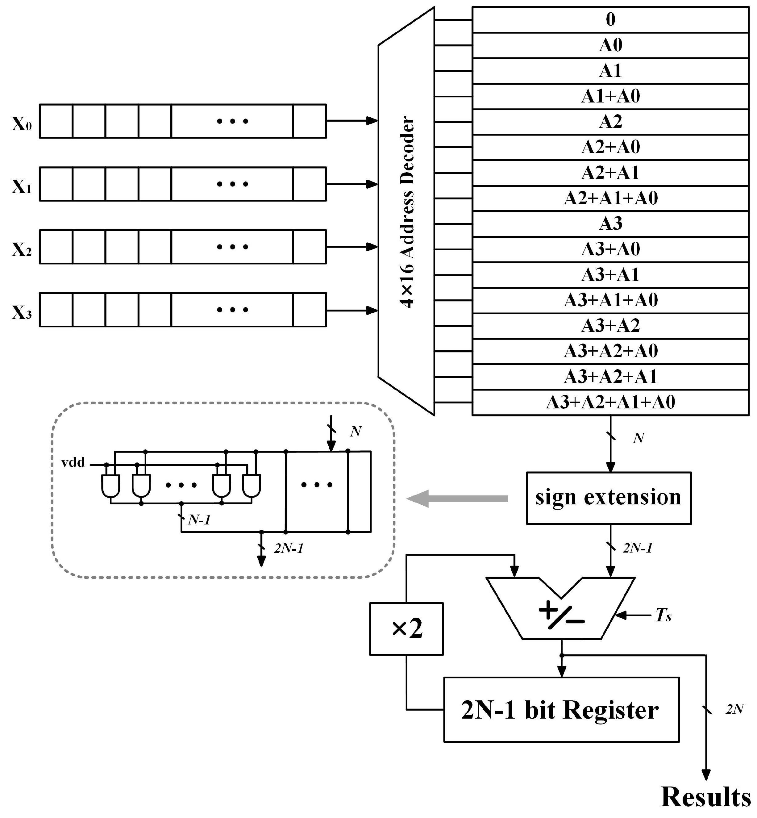
Figure 1 shows a detailed example of a DA computation. This structure consists of a look-up table with bits, each of the look-up table entries has corresponding registers storing input data, which are repackaged to form the memory address, most significant bit (MSB) first. The low right shows a sign extension block and -bit accumulator. The N-bit data fetched from the look-up table is scaled to -bit with -bit sign extension. The accumulation register adds two times of its previous value to the current look-up table contents every clock cycle. The signal is activated when the read-only memory (ROM) is addressed by the first bit of input data (sign). In this case, the adder subtracts the current ROM contents from the accumulator state. After N clock cycles, the -bit computation result is generated.
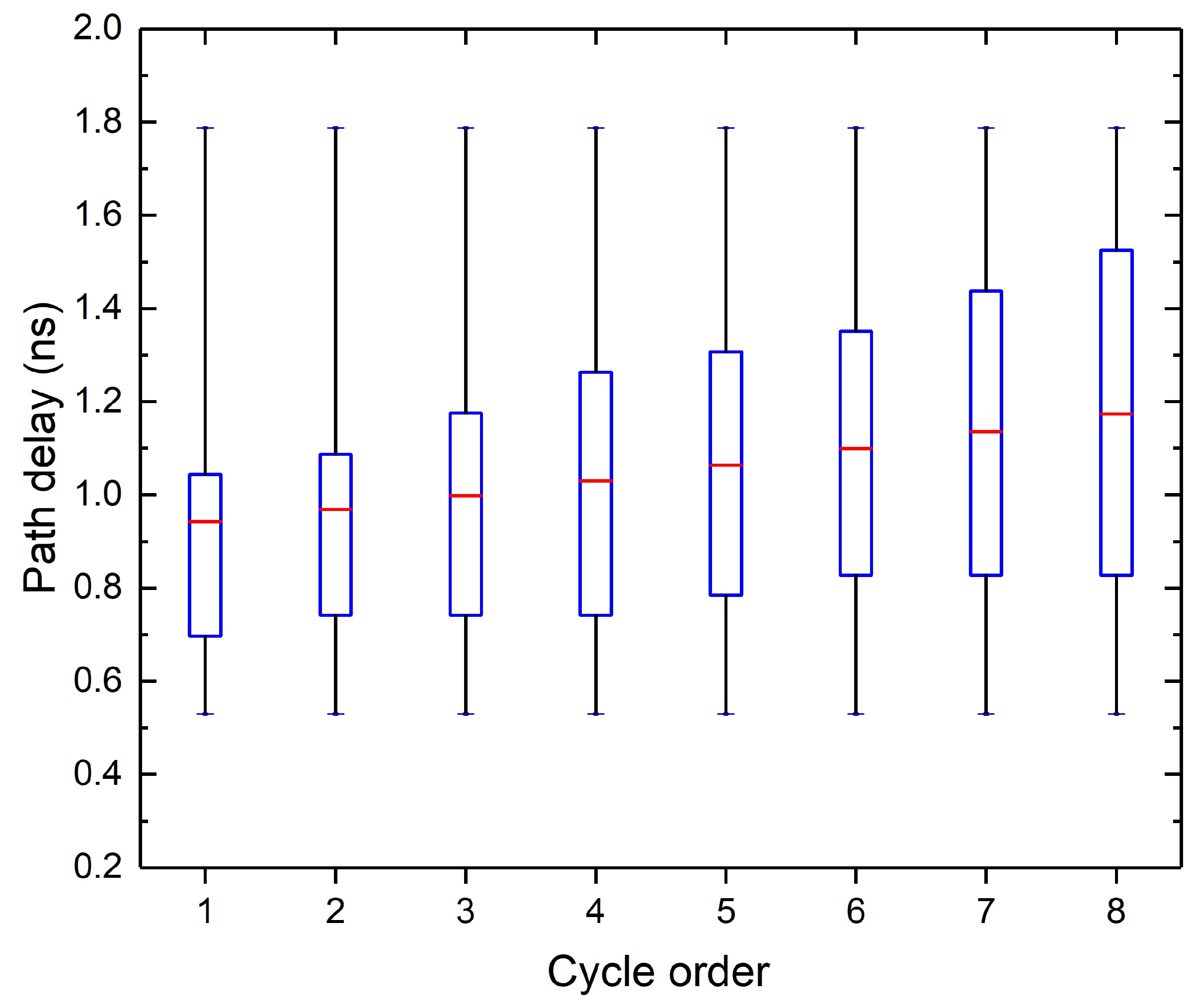
As the DA computation is realized using the same arithmetic unit in each clock cycle, delay imbalance of the DA circuit is very close, which significantly differs from the conventional arithmetic circuits. Figure 2 shows the results of a static timing analysis. The longest and fastest path delay for each cycle is almost same and the difference between the mean path delay is very tiny.
3. Proposed Variation-Aware DA Computation
The above observations show us that the DA circuit consumes various clock cycles to generate the result bit in order and the corresponding critical path in each cycle has a very small delay difference. Based on this characteristic, we propose to trade a small amount of area overheads to increase the difference between the critical (corresponds to the LSB computation) and other paths, thereby bounding the magnitude of timing errors with the presence of variations.
3.1. Dynamic Sign Extension
The proposed approach relies on achieving a small guard-band between the critical path delay in the different clock cycles, this is firstly realized by modification of the sign extension block. As described in Section 2, the sign extension block is used to scale the N-bit data to -bit for the further shift accumulation. Since the -bit shift accumulation involves significant path delay every clock cycle, the delay difference is negligible in the conventional DA design. In order to create the expected delay imbalance, a dynamic sign extension block is proposed.
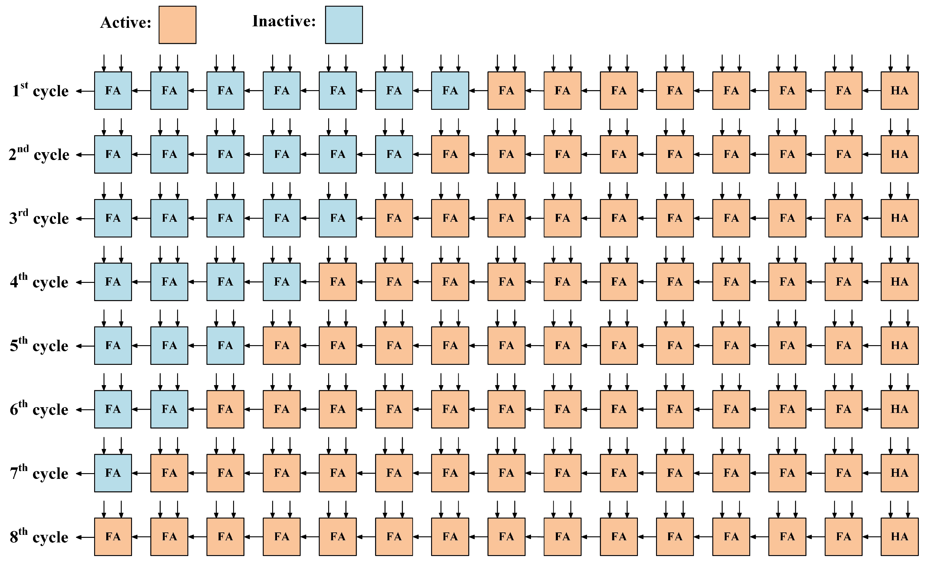
It can be found that only one increment bit is generated at each stage of the accumulation. Hence, there is no need to implement -bit accumulation every cycle. If the bit-width of the accumulate operation can be extended in sequence, the redundant additions can be avoided. To better illustrate, the accumulator circuit for an 8-bit DA computation can be seen in Figure 3. In the first cycle, the 8-bit ROM content is subtracted from zero and the result is stored in the registers, while the correct results would be acquired by a 15-bit addition in the eighth cycle.
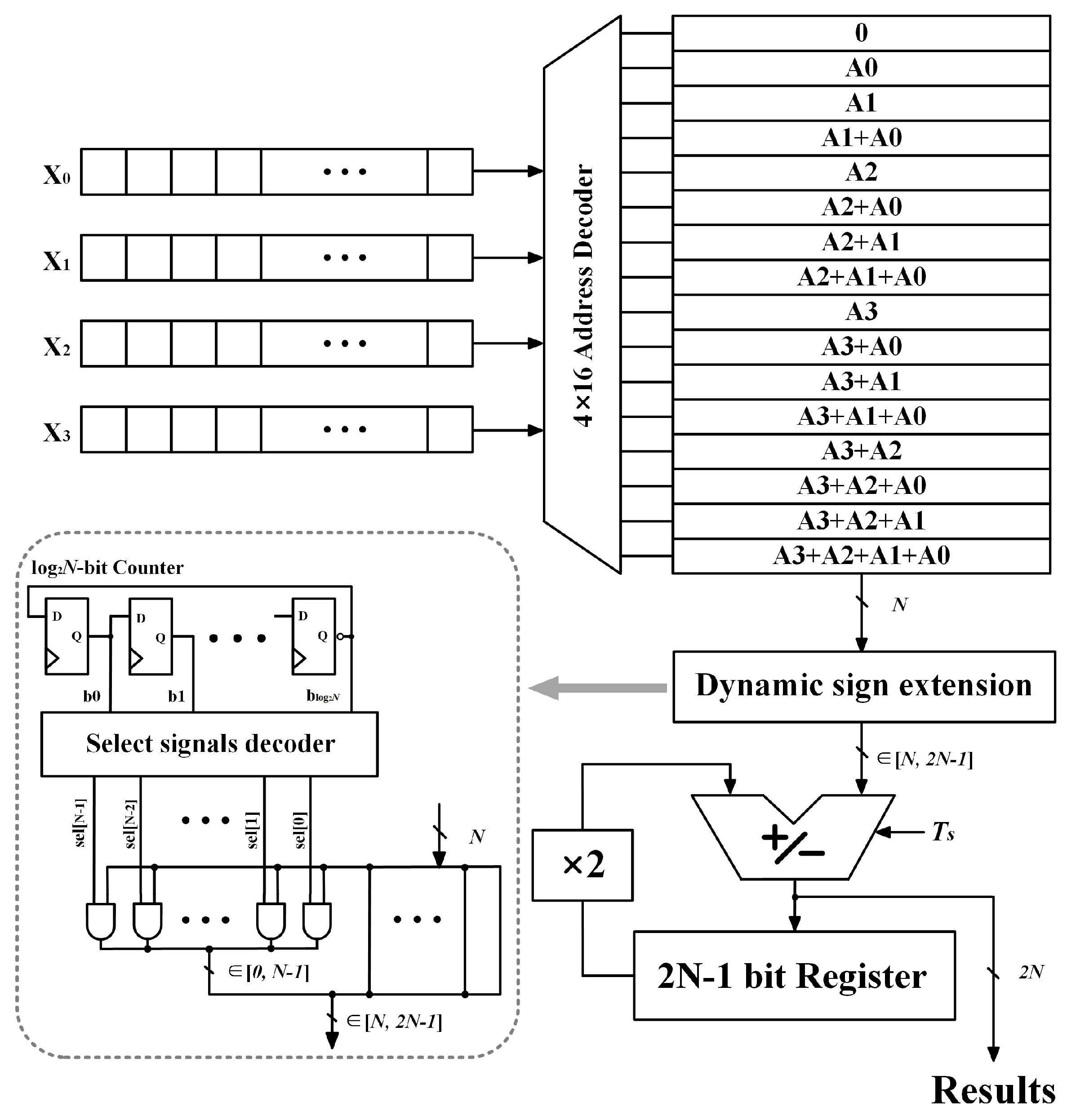
The VLSI implementation of the proposed DA circuit can be seen in Figure 4. A -bit counter is used to record the cycle order, the counter signals are fed into a decoder block in parallel to generate an -bit output signal named . The logic function of the proposed decoder can be realized by several combinational logic gates and clearly illustrated by an 8-bit case study as shown in Table 1. Each bit of the signal is connected to an individual AND gate respectively, while another input of theses gates is the sign bit of the current lookup-table content. Therefore, the signal can activate the extended sign bit during each clock cycle, until the final cycle, the fetched data would be scaled to -bit.
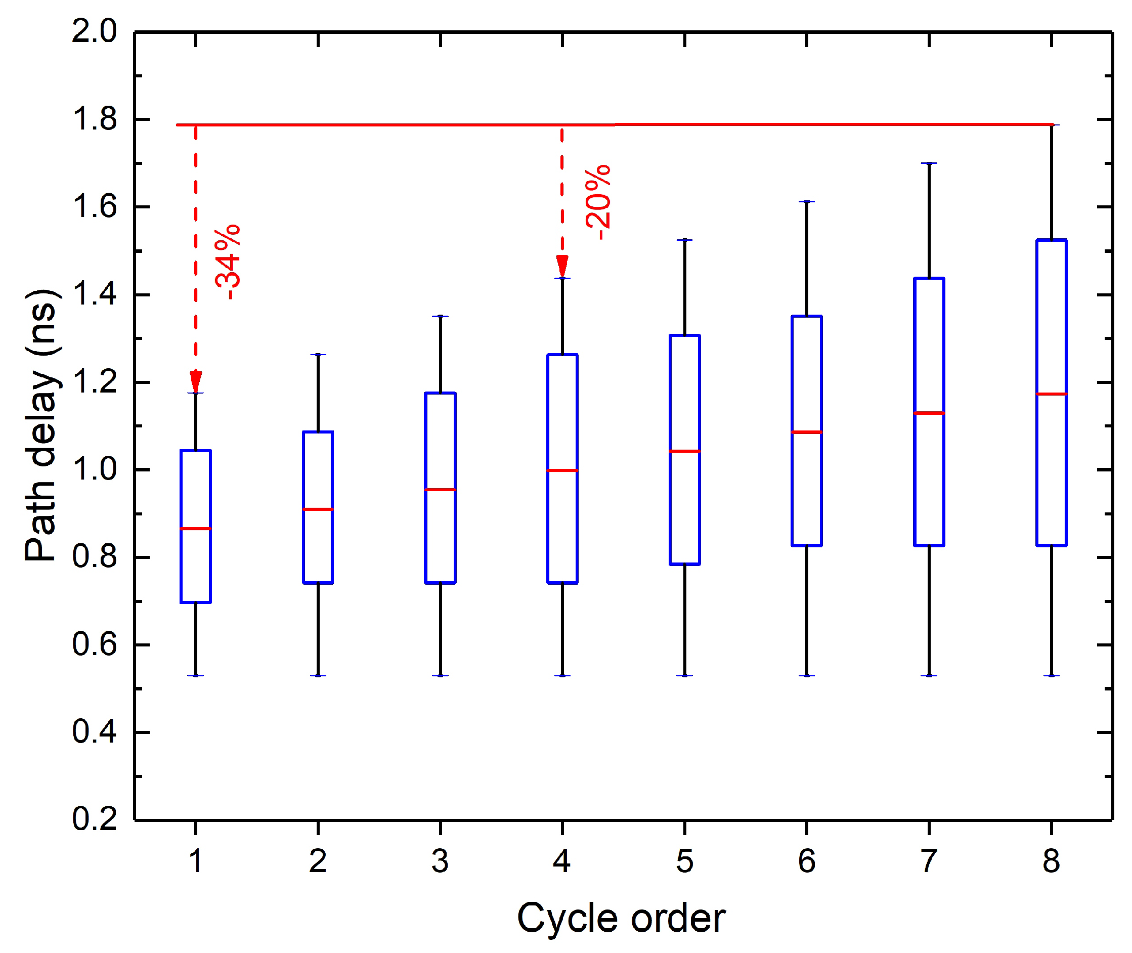
The modification in the circuit block alter the path delay distribution, the critical path delay increases linearly along with the cycle order, as shown in Figure 5. The largest delay difference can reach up to 0.78 ns, which is nearly a reduction.
3.2. Synthesis for Further Altering Path Delay Distribution
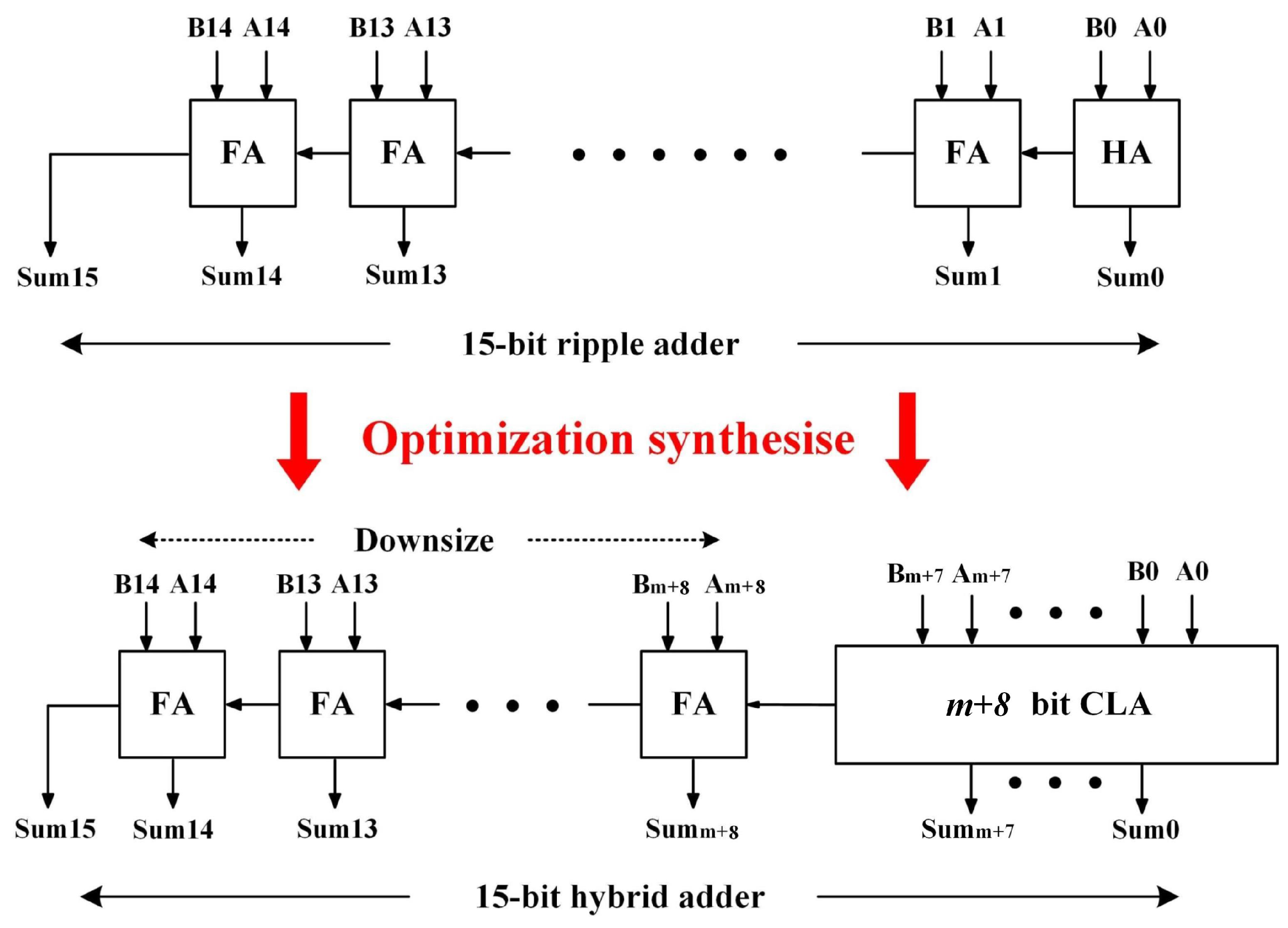
In the previous section, we proposed a dynamic sign extension block to create the delay imbalance. The next step is to further alter the path delay distribution at the synthesis level. The main idea is to replace some of the ripple adders by faster alternatives, such as carry-lookahead adders (CLA) and to realize the least area overhead by downsizing the rest ripple adders.
Assume an 8-bit DA circuit is required to have an -bit multiplication accuracy. In such a case, any bit errors occurring on the most significant m bits of the result, due to the variability, are considered to be unacceptable. We denote the most significant m bits as MSB. We then give MSB and MSB as the most and the least significant bits of MSB, respectively. As the errors are generally caused by the timing violations, a preset timing margin ( n% of the current circuit delay) can be applied to compensate for the possible timing variations. We propose a synthesis method, presented in Algorithm 1, to ensure a desired accuracy for a DA circuit, considering the possible variations. Specifically, a required circuit delay () is firstly computed based on the maximum delay that may cause timing violations, and the preset timing margin, n%. As has been described, a longer signal path is constructed for the computation of a less significant bit, allowing that the results of the more significant bits take the precedence to be produced. In this way, if the arrival time of MSB is not greater than , we can conclude that the arrival times of all bits of MSB are not greater than , and thus have more than n% timing margin. For this reason, we only evaluate the arrival time of MSB, denoted as t, in the following steps. The optimization process is initiated if t is larger than the required delay, . Two phases are included in the optimization process: adder replacement and gate downsizing.
| Algorithm 1 Synthesis for accuracy specification |
| Require: the arrival times of MSB have more than n% timing margin; procedure syn() max delay/(1+n%); signal arrival time of MSB; // Adder replacement if then all ripple adders on the critical path ending at MSB; 2; ▹ the number of 1-bit adders that can be replaced by a CLA repeat Replace i 1-bit adders of by a CLA i increases; until ; // Gate downsizing all gates that are irrelevant to MSB; Downsize . |
During the adder replacement phase, the ripple adder located at the critical path arriving at MSB are replaced by a CLA. A ripple adder consists of number of 1-bit adders and we denote all 1-bit adders of a ripple adder as . Here we partially replace the ripple adder to find the design with the least area increase satisfying . Thus, the optimization starts by replacing the least number of the 1-bit adders. In this case, we assume the least number of the 1-bit adders that can be replaced by a CLA is two, while it could be different based on the minimum length of a CLA provided in a library. Afterwards, the arrival time of MSB on the replaced critical path is checked: if t is still larger than , the number of i is increased, indicating more 1-bit adders would be replaced by a CLA. The above steps are repeated until t becomes less than or equal to , which suggests the arrival times of all bits of MSB have more than n% timing margins.
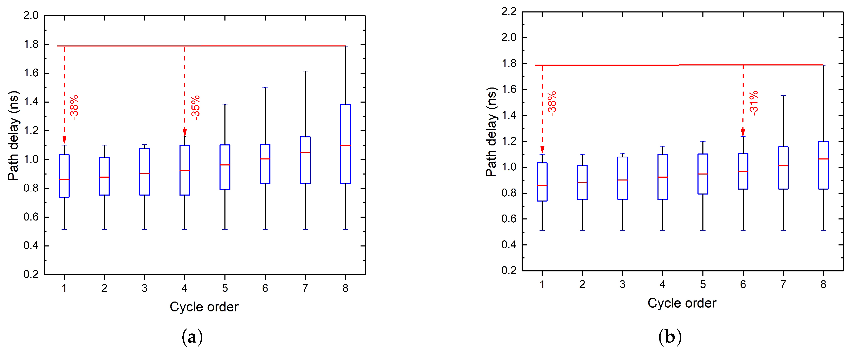
By replacing the ripple adders with CLAs, the overall area of the circuit is increased. The area overhead can be reduced by downsizing some gates that do not affect the circuit accuracy. For instance, according to Figure 6, a 15-bit accumulator is required for an 8-bit computation, where m full adders are inactive when computing the most significant bits. In such a case, these m adders can be downsized while the circuit can still at least obtain an -bit accuracy. Thus, during the gate downsizing phase, we firstly identify the inactive gates based the given accuracy specification. We denote as all gates that do not affect the result of MSB. The gates of are then replaced by those having the same functions but smaller dimensions. Accordingly, the path delay distribution can be modified with the synthesis approach, example cases with and are presented in Figure 7.
4. Case Study: FIR Filter VLSI Implementation
As mentioned in the previous section, the proposed approach can improve circuit robustness against timing errors at the cost of hardware area. To demonstrate this, the proposed architecture was applied on a digital FIR filter. This design is synthesized using the Synopsys Design Compiler with the ST 65 nm CMOS process.
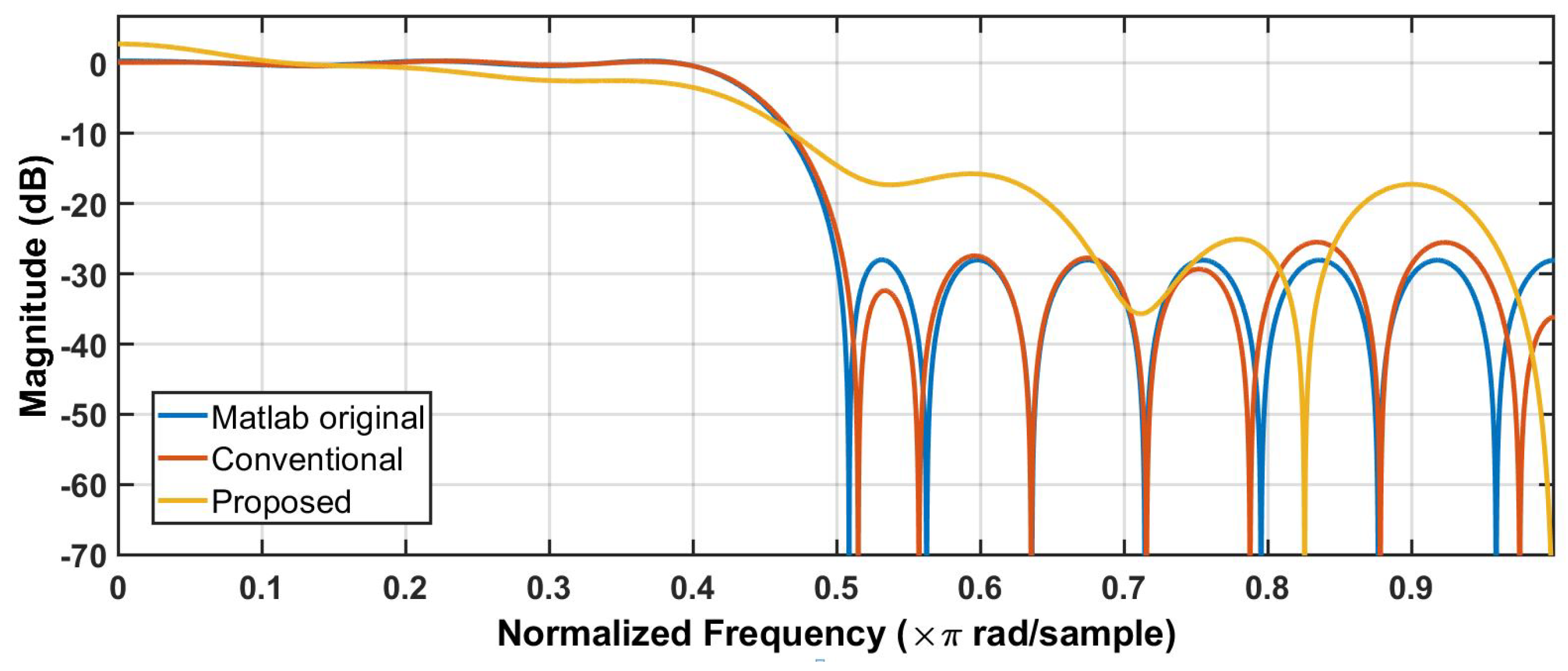
We synthesize the FIR filter with the following coefficient set {−0.0215, 0.0106, 0.0270, 0.0084, −0.0261, −0.0147, 0.0390, 0.04225, −0.04285, −0.0905, 0.0490, 0.3138, 0.4507, 0.3138, 0.0490, −0.0905, −0.0428, 0.0422, 0.0390, −0.0147, −0.0261, 0.0084, 0.0270, 0.0105, −0.0215}. Both the proposed DA-based and conventional designs are simulated in the worst case (slow corner, 125C) without any timing margin. The corresponding filter characteristics are shown in Figure 8, compared with the magnitude response of the original floating-point filter. The simulation results show that our proposed design can maintain an approximately correct function while the conventional design suffers from significant accuracy loss. In this design, the proposed approach trades extra hardware cost for error resilience over a given timing guard-band. For a 16-tap implementation, this approach results in approximately extra hardware area.
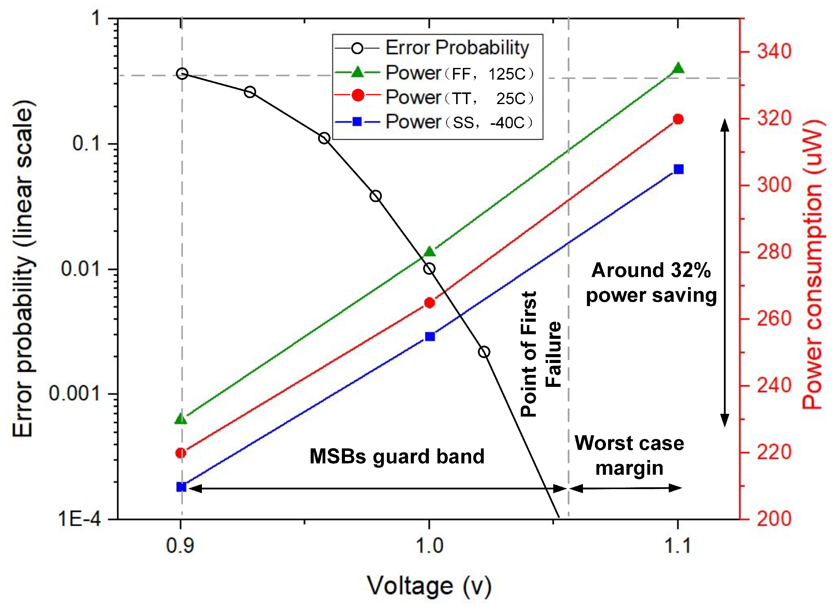
Because the simulation results of power consumption and computation accuracy are dependent on the input samples and the coefficients, random stimulus is implemented over the full input dynamic range. The power consumption savings in our proposed FIR filter are shown in Figure 9 under different circumstances of slow-slow (SS), typical-typical (TT), fast-fast (FF) corners, and −40 C, 25 C, 125 C. Compared with the TT process corner, 25 C, and 1.2 V supply voltage, the proposed approach achieves , , and power savings for best (SS corner, −40 C), nominal (TT corner, 25 C) and worst (FF corner, 125 C) cases, respectively (at 1.00 V). When the voltage is reduced to 0.90 V, a maximum power reduction of up to can be obtained. To better present the trade-off between the power consumption and computation accuracy, the error probability () serves as the measurement metric to evaluate the accuracy loss, which means it is probable that the output of computation differs from the correct one. Figure 9 also shows the error probability versus supply voltage, starting from the nominal 1.10 V, which includes the full worst-case design margin. If this margin is removed in the nominal case (TT, 25 C) using DVS, high-accuracy operations can still be retained. The point of first failure (PoFF) occurs at 1.06 V, where the paths from the LSB group start to fail, but the corresponding error rate is extremely low. Beyond 0.90 V, MSBs paths also begin to fail, which leads to a rapid decline in computation accuracy.
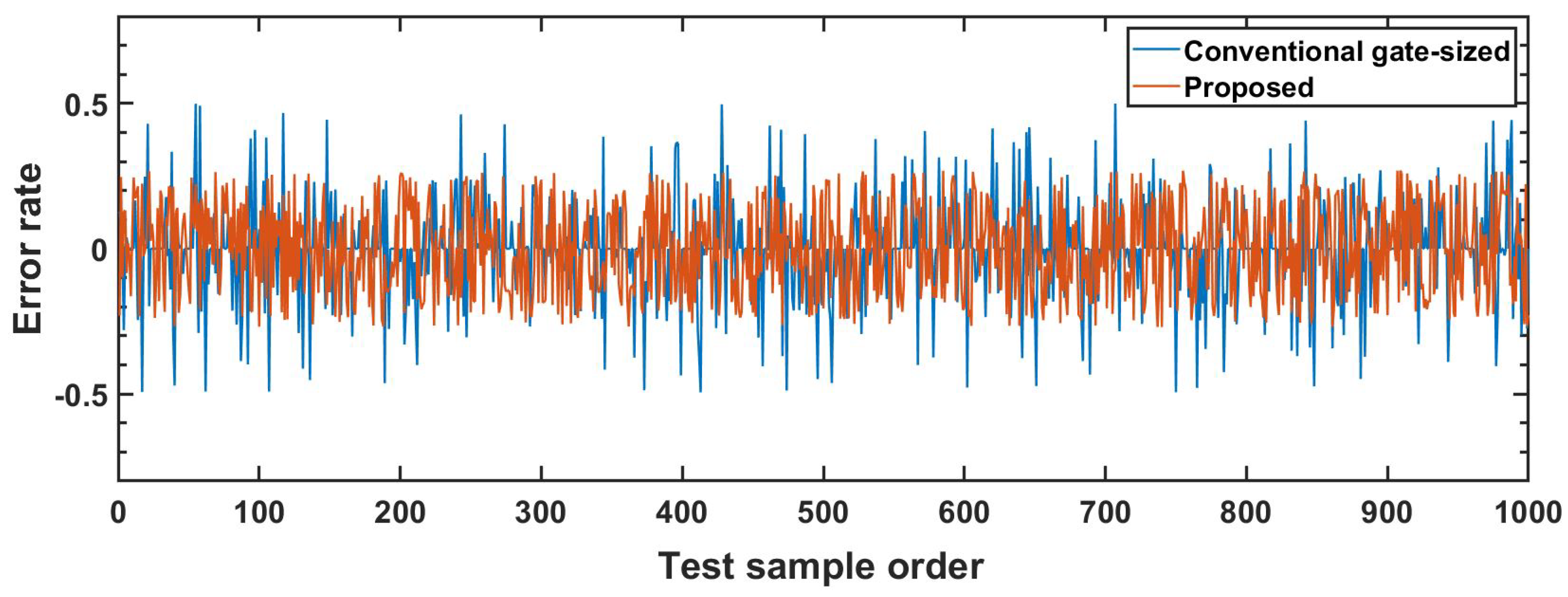
To implement a tentative comparison, the conventional DA-based design is up-sized to achieve the same hardware cost as the proposed one. Hence, more timing guardband is provided via gate sizing for the conventional design. The error rate comparison between the gate-sized conventional and proposed design with 0.9 V supply voltage using 1000 test samples can be seen in Figure 10. The conventional gate-sized design would suffer from more than accuracy loss some time while at least computation accuracy can still remain using the proposed error-mitigation method.
5. Conclusions
In this paper, a novel approach to distributed arithmetic (DA) is proposed to mitigate the effects of process, voltage, and temperature (PVT) variations. The bit-slice accumulation of DA is modified as MSB-first, it can alter the path delay distribution, where the MSB path has the shortest delay. Additionally, extra timing slack is provided for computations of the MSB group by a modified sign extension block and carefully gate-sizing, thereby providing extra guardband against the variation-induced timing violations. A case study of FIR implementation shows that this design outperforms the traditional gate-sized counterpart in terms of computation accuracy with the same hardware overhead () while it can also achieve significant power savings up to under different operating conditions when the worst case margin is included.
Author Contributions
Y.L. and S.D. designed, simulated and measured the circuits described in this manuscript under the supervision of T.K., and B.H contributed to the technical discussions during the design time.
Funding
This research received no external funding.
Acknowledgments
The authors would like to thank Mengjia Ye and Park Lu, for partially supporting this work.
Conflicts of Interest
The authors declare no conflict of interest.
References
- Muhic, I.; Hodzic, M. Internet of Things: Current Technological Review and New Low Power Wireless Sensor Network Protocol Proposal. Southeast Eur. J. Soft Comput. 2014, 3. [Google Scholar] [CrossRef] [Green Version]
- Gubbi, J.; Buyya, R.; Marusic, S.; Palaniswami, M. Internet of Things (IoT): A vision, architectural elements, and future directions. Future Gener. Comput. Syst. 2013, 29, 1645–1660. [Google Scholar] [CrossRef] [Green Version]
- Golanbari, M.S.; Tahoori, M.B. Runtime adjustment of IoT system-on-chips for minimum energy operation. In Proceedings of the 55th Annual Design Automation Conference, San Francisco, CA, USA, 24–28 June 2018; p. 145. [Google Scholar]
- Kiamehr, S.; Ebrahimi, M.; Golanbari, M.S.; Tahoori, M.B. Temperature-aware dynamic voltage scaling to improve energy efficiency of near-threshold computing. IEEE Trans. Very Large Scale Integr. Syst. 2017, 25, 2017–2026. [Google Scholar] [CrossRef]
- Licciardo, G.D.; Cappetta, C.; Di Benedetto, L.; Vigliar, M. Weighted Partitioning for Fast Multiplierless Multiple-Constant Convolution Circuit. IEEE Trans. Circuits Syst. II Express Briefs 2017, 64, 66–70. [Google Scholar] [CrossRef]
- Panwar, M.; Padmini, J.; Acharyya, A.; Biswas, D. Modified distributed arithmetic based low complexity CNN architecture design methodology. In Proceedings of the 2017 European Conference on Circuit Theory and Design (ECCTD), Catania, Italy, 4–6 September 2017; pp. 1–4. [Google Scholar]
- Xie, J.; Meher, P.K.; He, J. Hardware-efficient realization of prime-length DCT based on distributed arithmetic. IEEE Trans. Comput. 2013, 62, 1170–1178. [Google Scholar] [CrossRef]
- Martina, M.; Masera, G.; Roch, M.R.; Piccinini, G. Result-biased Distributed-Arithmetic-based filter architectures for approximately computing the DWT. IEEE Trans. Circuits Syst. I Reg. Pap. 2015, 62, 2103–2113. [Google Scholar] [CrossRef]
- Singhal, S.K.; Mohanty, B.K. Efficient Parallel Architecture for Fixed-Coefficient and Variable-Coefficient FIR Filters Using Distributed Arithmetic. J. Circuits Syst. Comput. 2016, 25, 1650073. [Google Scholar] [CrossRef]
- Park, S.Y.; Meher, P.K. Low-power, high-throughput, and low-area adaptive FIR filter based on distributed arithmetic. IEEE Trans. Circuits Syst. II Express Briefs 2013, 60, 346–350. [Google Scholar] [CrossRef]
- Venkatachalam, S.; Ko, S.B. Approximate Sum-of-Products Designs Based on Distributed Arithmetic. IEEE Trans. Very Large Scale Integr. Syst. 2018, 26, 1604–1608. [Google Scholar] [CrossRef]
- Mittal, S. A survey of techniques for approximate computing. ACM Comput. Surv. 2016, 48, 62. [Google Scholar] [CrossRef]
- Radfar, M.; Singh, J. A yield improvement technique in severe process, voltage, and temperature variations and extreme voltage scaling. Microelectron. Reliab. 2014, 54, 2813–2823. [Google Scholar] [CrossRef]
- Islam, A.; Hasan, M. A technique to mitigate impact of process, voltage and temperature variations on design metrics of SRAM Cell. Microelectron. Reliab. 2012, 52, 405–411. [Google Scholar] [CrossRef]
- Golanbari, M.S.; Gebregiorgis, A.; Moradi, E.; Kiamehr, S.; Tahoori, M.B. Balancing resiliency and energy efficiency of functional units in ultra-low power systems. In Proceedings of the 23rd Asia and South Pacific Design Automation Conference, Jeju, Korea, 22–25 January 2018; pp. 637–644. [Google Scholar]
- Khairy, M.S.; Gholamipour, A.; Kurdahi, F.J.; Eltawil, A.M. Reliable low power Distributed Arithmetic filters via N-Modular Redundancy. In Proceedings of the 2012 Conference Record of the Forty Sixth Asilomar Conference on Signals, Systems and Computers (ASILOMAR), Pacific Grove, CA, USA, 4–7 November 2012; pp. 621–625. [Google Scholar]
- Ting, Y.H.; Lin, T.J.; Chang, C.C.; Hu, C.C.; Yeh, C.; Wang, J.S. Approximate Distributed Arithmetic for Variable-Latency Table Lookup. In Proceedings of the 2017 New Generation of CAS (NGCAS), Genova, Genoa, 6–9 September 2017; pp. 137–140. [Google Scholar] [CrossRef]
- Alam, M. Reliability-and process-variation aware design of integrated circuits. Microelectron. Reliab. 2008, 48, 1114–1122. [Google Scholar] [CrossRef]
- Zhang, S.; Shanbhag, N.R. Embedded algorithmic noise-tolerance for signal processing and machine learning systems via Data Path Decomposition. IEEE Trans. Signal Process. 2016, 64, 3338–3350. [Google Scholar] [CrossRef]
- Vaseghi, S.V. Advanced Digital Signal Processing and Noise Reduction; John Wiley & Sons: Chichester, West Sussex, UK; 2008; ISBN 978-0-470-75406-1. [Google Scholar]
- Ernst, D.; Kim, N.S.; Das, S.; Pant, S.; Rao, R.; Pham, T.; Ziesler, C.; Blaauw, D.; Austin, T.; Flautner, K.; et al. Razor: A low-power pipeline based on circuit-level timing speculation. In Proceedings of the 36th Annual IEEE/ACM International Symposium on Microarchitecture, Washington, DC, USA, 3–5 December 2003; p. 7. [Google Scholar]
- Choi, J.H.; Banerjee, N.; Roy, K. Variation-aware low-power synthesis methodology for fixed-point FIR filters. IEEE Trans. Comput.-Aided Des. Integr. Circuits Syst. 2009, 28, 87–97. [Google Scholar] [CrossRef]
- Whatmough, P.N.; Das, S.; Bull, D.M.; Darwazeh, I. Circuit-level timing error tolerance for low-power DSP filters and transforms. IEEE Trans. Very Large Scale Integr. Syst. 2013, 21, 989–999. [Google Scholar] [CrossRef]
- Tiwari, A.; Sarangi, S.R.; Torrellas, J. ReCycle: Pipeline Adaptation to Tolerate Process Variation; ACM SIGARCH Computer Architecture News; ACM: New York, NY, USA, 2007; Volume 35, pp. 323–334. [Google Scholar]
Figure 1.
Conventional most significant bit (MSB)-first distributed arithmetic ROM and accumulator (RAC) structure.
Figure 1.
Conventional most significant bit (MSB)-first distributed arithmetic ROM and accumulator (RAC) structure.

Figure 2.
Distribution of path delay in each clock cycle.

Figure 3.
The state change of full adder in the accumulator circuit for an 8-bit distributed arithmetic (DA) computation.
Figure 3.
The state change of full adder in the accumulator circuit for an 8-bit distributed arithmetic (DA) computation.

Figure 4.
DA circuit with the modified dynamic sign extension block.

Figure 5.
Distribution of path delay in each clock cycle with the proposed dynamic sign extension block.
Figure 5.
Distribution of path delay in each clock cycle with the proposed dynamic sign extension block.

Figure 6.
An example of the proposed synthesis approach.

Figure 7.
Distribution of path delay in each clock cycle with synthesis optimization, when (a) m = 4 (b) m = 6.
Figure 7.
Distribution of path delay in each clock cycle with synthesis optimization, when (a) m = 4 (b) m = 6.

Figure 8.
Frequency response of conventional design versus proposed design in the worst case (slow-slow (SS) process corner and 125 C temperature).
Figure 8.
Frequency response of conventional design versus proposed design in the worst case (slow-slow (SS) process corner and 125 C temperature).

Figure 9.
Power dissipation and error probability versus supply voltage with different process corners and temperature.
Figure 9.
Power dissipation and error probability versus supply voltage with different process corners and temperature.

Figure 10.
The error rate comparisons between the gate-sized conventional and proposed design with 0.9 V supply voltage using 1000 test samples.
Figure 10.
The error rate comparisons between the gate-sized conventional and proposed design with 0.9 V supply voltage using 1000 test samples.


Table 1.
Binary representation of the signals and along with the cycle order.
| Cycle Order | Counter () | Signal Select [6:0] | Select [Cycle Order − 1] |
|---|---|---|---|
| 1 | 000 | 0000000 | |
| 2 | 001 | 0000001 | |
| 3 | 010 | 0000011 | |
| 4 | 011 | 0000111 | |
| 5 | 100 | 0001111 | |
| 6 | 101 | 0011111 | |
| 7 | 110 | 0111111 | |
| 8 | 111 | 1111111 |
© 2019 by the authors. Licensee MDPI, Basel, Switzerland. This article is an open access article distributed under the terms and conditions of the Creative Commons Attribution (CC BY) license (http://creativecommons.org/licenses/by/4.0/).
Share and Cite
MDPI and ACS Style
Lu, Y.; Duan, S.; Halak, B.; Kazmierski, T. A Variation-Aware Design Methodology for Distributed Arithmetic. Electronics 2019, 8, 108. https://doi.org/10.3390/electronics8010108
AMA Style
Lu Y, Duan S, Halak B, Kazmierski T. A Variation-Aware Design Methodology for Distributed Arithmetic. Electronics. 2019; 8(1):108. https://doi.org/10.3390/electronics8010108
Chicago/Turabian StyleLu, Yue, Shengyu Duan, Basel Halak, and Tom Kazmierski. 2019. "A Variation-Aware Design Methodology for Distributed Arithmetic" Electronics 8, no. 1: 108. https://doi.org/10.3390/electronics8010108
Note that from the first issue of 2016, this journal uses article numbers instead of page numbers. See further details here.